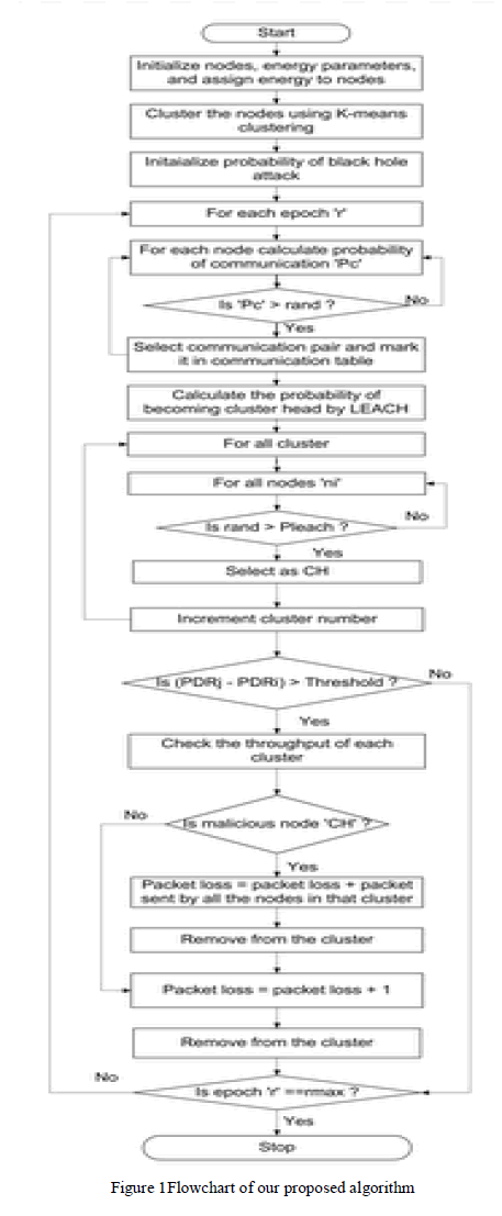
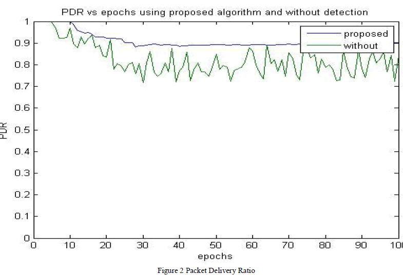
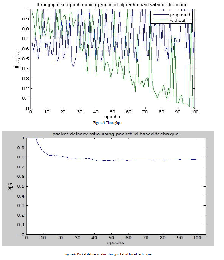
International Journal of Innovative Research in Science, Engineering and Technology
ISSN ONLINE(2319-8753)PRINT(2347-6710)
ISSN ONLINE(2319-8753)PRINT(2347-6710)
Nancy.R 1, Radhalakshmi.K2
|
| Related article at Pubmed, Scholar Google |
Visit for more related articles at International Journal of Innovative Research in Science, Engineering and Technology
In this paper, a high step-up converter using coupled inductor with Fuzzy Logic Control is analyzed and simulated. The converter uses a coupled inductor and a switched capacitor circuit to achieve high voltage conversion ratio. Two capacitors and diodes constitute the switched capacitor circuit. The two capacitors are charged in parallel during the switch-off period and are discharged in series during the switch-on period by the energy stored in the coupled inductor to achieve a high step-up voltage gain. Switch voltage stress and the circulating current are reduced by a clamp circuit which is composed of a diode followed by a capacitor. Thus the efficiency of the converter is improved. The operating principle and the steady state analysis are discussed in detail. A Fuzzy logic controller is designed such that it eliminates the Voltage Drift problem.
Keywords |
| Coupled Inductor, FLC, Switched Capacitor circuit. |
INTRODUCTION |
| Renewable energy sources (RES) have experienced a fast development in recent years. These systems employ with micro sources like PV, fuel cells etc. Though PV cells can be made into array and connected in series to produce high voltage there exist serious problems like shadowing effects, short circuit which drastically reduces its efficiency. In order to overcome such adverse effects this micro source energy is utilized by the high step up converter to produce high voltage and satisfy the demands. Conventional boost converters can’t provide such a high DC voltage gain for extreme duty cycle. Thus high step up dc-dc converters are used as front end converters to step from low voltage to high voltage which are required to have a large conversion ratio, high efficiency and small volume [1].In some converters active clamp circuit is used to overcome voltage spikes caused by the leakage inductance of the coupled inductor. Though ZVS technique is employed for soft switching it can’t sustain light loads [2].Different switching structures are formed either two capacitor or two inductor with twothree diodes. Both the step up and step down operations can be performed in this topology, Performance of hybrid converters are better than classical converters but still its costlier to implement [3]. Low level voltage from the PV, fuel cells is connected to Kilo watt level using step up dcdc converter and inverter circuits. Voltage spikes and switching losses are eliminated by active clamping. In dc-ac, inverter always tends to draw ac ripple current at twice the output frequency. Resonant inductors cost and circuit volume is high [4]. In some converters high voltage conversion is obtained by changing transformer turns ratio which will increase the overall efficiency but still the operation of main switch involves hard switching and also EMI noise gets raised [5]. Impacts of SiC (silicon carbide) MOSFETS on converter, switching and conduction losses are reduced even though fast switching is done. Si diodes have ideal, but sill SiC devices processes large amount of ringing current at turn OFF relatively to other devices. Package of external diode and the diode itself have more parasitic capacitances that are added to the devices parasitic aggravating the ringing [6].Here, the voltage step is done without a transformer and a high voltage gain s achieved without an extremely high duty ratio but still the circuit becomes more bulky as more number of passive components are used [7]. Though this converter provides a non-pulsating current by using an auto transformer, duty ratio is limited by 0.5 and not suitable for non-linear loads [8].Here voltage stress of the active switch is reduced thereby the conversion efficiency is improved. This converter requires a multi winding transformer which makes the circuit design complex [9]. This converter avoids extremely narrow turn off period, ripples and switching losses are eliminated by ZVS technique. It uses two coupled inductors which makes the circuit complex [10]. In this converter no additional magnetic components used, switching losses are minimized by adopting a regenerative snubber circuit. As the circuit uses more switches controlling is complex [11]. In this converter high voltage gain is obtained but the circuit has more passive components [12]. It employees single ended scheme cost is reduced. Galvanic isolation is needed, but suitable only for low power and frequency applications [13], [14]. In this converter no need of extreme duty ratio but if conduction losses or switching losses occurs the efficiency is reduced [15]. It is possible to generate the non-isolated dc-dc converters but the major drawback is that switching frequency must be maintained constant and the turn ratio of the auto transformer must be unity [16]. Some converters operate at very high frequency with fast transient response. The main switch is fabricated from an integrated power process, the layouts can be changed to vary the parasitic, however design of switch layout is complex, fixed frequency and constant duty ratio must be maintained [17]. This converter provides high voltage gain and can be employed for high power applications however the duty ratio is limited to 0.85 [18], [19]. In this, the energy of the leakage inductor is recycled to the output load directly, limiting the voltage spike on the main switch. To achieve a high step-up gain, it has been proposed that the secondary side of the coupled inductor can be used as flyback and forward converters [20], [21].In some converters voltage gain is improved through output voltage stacking [22]. |
 |
| The main objective is to improve the Voltage Gain of the Step-up Converter and also to reduce Voltage stress of the circuit. Further the Voltage Drift problem is reduced using closed loop control of the proposed converter with fuzzy logic controller. From Fig.1, The output voltage from the converter is fed as feed back to the FLC; there it compares the feedback voltage signal and the reference voltage signal to produce PWM pulse which triggers the main switch of the converter. |
OPERATING PRINCIPLE OF THE PROPOSED CONVERTER |
| Fig. 2 shows the circuit configuration of the proposed converter, which consists of a boost converter, coupled inductor, switched capacitor circuit and a clamp circuit. The equivalent circuit of the coupled inductor has a magnetizing inductor Lm, leakage inductor Lk, and an ideal transformer. Ns and Np is the primary and secondary winding of theideal transformer,Vin DC input voltage, V0 is the DC output voltage, and S main switch. |
 |
| The diodes D2, D3 and capacitors C2, C3 forms the switched capacitor circuit. D1, C1 are the clamp diode and clamp capacitor respectively. The operating principle is that when the switch S is ON, the input supply voltage charges the magnetizing inductor Lm which is in the primary side of the coupled inductor Np. This Np induces emf to the secondary side of the coupled inductor which makes the capacitors C1, C2, C3 to discharge in series and delivers to the load resistance. The output capacitor C0 is in charging state. When the switch S is turned OFF, the energy stored in the magnetizing inductor gets discharged and makes the capacitors C2, C3 to charge in parallel. Meanwhile, the D1 is turned ON and charges the clamp capacitor C1, thus reduces the switch voltage stress and the circulating current. The energy stored in C0 is delivered to the load resistance. Fig. 3 shows the typical waveforms. |
 |
| Assumptions to simplify the circuit analysis, |
| 1. Capacitors C1, C2, C3 and C0 are large enough. And so, VC1, VC2, VC3 and VC0 are considered as constants in one switching period. |
| 2. The power devices are ideal. |
| 3. The coupling coefficient of the coupled inductor k is equal to Lm/ (Lm+Lk), and the turn ratio of the coupled inductor n is equal to Ns/Np. |
| A. Mode of Operation |
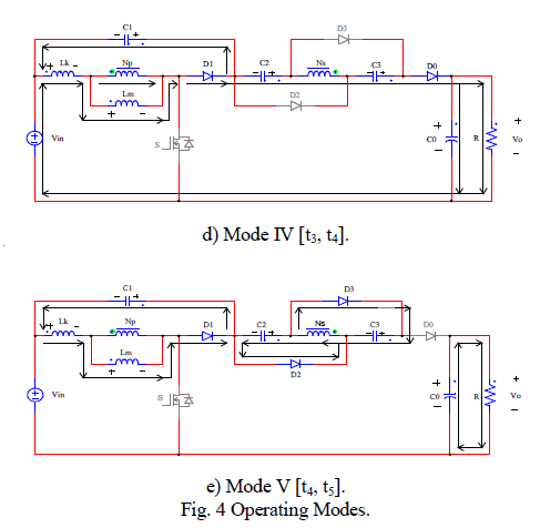
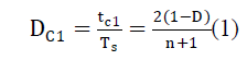
| There are five operating modes in one switching period. Fig. 4 shows the current-flow path of each mode of the circuit. |
| a) Mode I [t0, t1]: In this mode, S is turned on. Diodes D1 and D0are turned off, and D2 and D3 are turned on. The current-flow path is shown in fig. 4(a).The leakage inductor Lkchargedby Vin. Output capacitor C0provides its energy to load R.When current iD2 becomes zero at t = t1, this operating mode ends. |
| b) Mode II [t1, t2]: In this mode, S remains turned on. Diode D1, D2, and D3 are turned off and D0 is turned on.The current-flow path is shown in fig. 4(b).Magnetizing inductor Lmcharges by Vin. The induced voltage VL2 on the secondary side of the coupled inductor makes Vin, VC1, VC2and VC3, which are connected in series, discharge to high-voltage output capacitor C0 and load R. when switch S is turned off this mode ends. |
| c) Mode III [t2, t3]: In this mode, S is turned off. Diodes D1, D2, and D3 are turned off and D0 is turned on. The current-flow path is shown in fig. 4(c). The energies of Lk and Lm charge the parasitic capacitor Cdsof main switch S. Output capacitor C0 provides its energy to load R. At t = t3, diode D1 conducts, and this mode ends. |
| d) Mode IV [t3, t4]: In this mode, S is turned off. Diodes D1 and D0 are turned on, and D2 and D3 are turned off. The current-flow path is shown in fig. 4(d). The energies of Lk and Lm charge C1. The energy of Lk is recycled. Secondary-side voltage VL2 of the coupled inductor continues charging high-voltage output capacitor C0 and load R in series until the secondary current of the coupled inductor is equal to zero. At t = t4, this mode ends. |
| e) Mode V [t4, t5]: In this mode, S is turned off. Diode D1, D2, and D3 are turned on and D0 is turned off. The current-flow path is shown in fig. 4(e). C0 is discharged to load R. The energies of Lkand Lm charge the C1. Lm is released via the secondary side of the coupled inductor and charges capacitors C2 and C3. Thus, C2 and C3 are charged in parallel and Lk charges capacitor C1. This mode ends at t = t6. |
 |
 |
ANALYSIS OF THE PROPOSED CONVERTER |
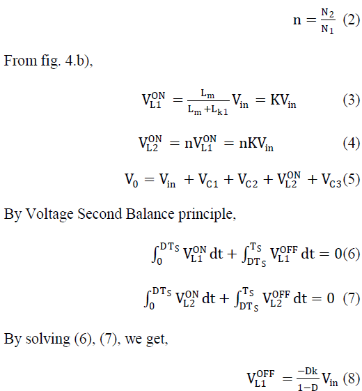
| According to [1], the energy stored in the leakage inductor Lkof the coupled inductor is released to capacitor C1. The energy-released duty cycle DC1 can be expressed as |
 |
| The equivalent circuit and state definition of the newly designed converter is depicted in fig.2, where the transformer is modeled as an ideal transformer. |
| The turn ratio of this ideal transformer is defined as |
 |
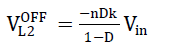 |
| As the capacitors are charged during switch OFF mode, the voltage across the capacitors can be obtained from fig.4(e), |
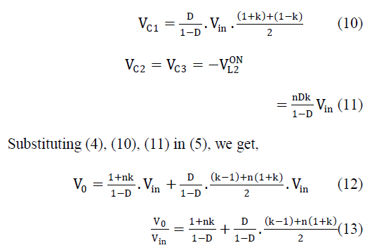 |
| According to the description of operating modes, voltage stresses on active switch Sand diodes D1, D2, D3, and D0are given as |
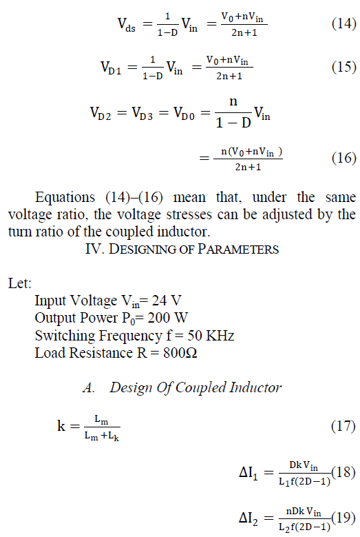 |
| From equations (13), (17), (18) & (19) the values of L1 =1.48mH, L2 = 5.62 mH are obtained. Here the Lm&Lk values are chosen as 48μH & 0.25μH. |
| B. Selection of Switching Device |
POWER MOSFET: |
| It is chosen as switch as it is cost effective, high commutation speed, low on state resistance, improved gate and high speed power switching. To verify the performance of the proposed converter, circuit is simulated using MATLAB software. The Converter specifications are as follows: |
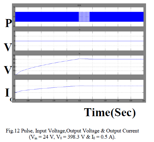
| 1) Input dc voltage Vin =24 V |
| 2) Output dc voltage V0 = 400 V |
| 3) Maximum output power P0 = 200 W |
| 4) Switching frequency f = 50 kHz |
| 5) Capacitors C1 = 56 μF |
| C2/C3 = 22 μF |
| C0 = 180 μF |
| 6) Coupled inductor n = Np:Ns= 1: 4 Lm&Lk = 48 μH& 0.25 μH |
FUZZY LOGIC CONTROLLER DESIGN |
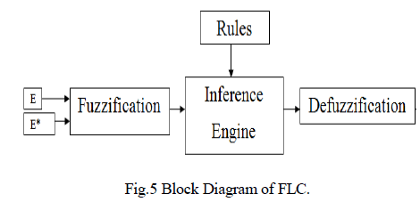
| The block diagram of fuzzy logic controller (FLC) is shown in fig.5. It consists of three main blocks: fuzzification, inference engine and defuzzification. The two FLC input variables are the error E and change in error E*. Depending on membership functions and the rules FLC operates. |
 |
| A. Fuzzification |
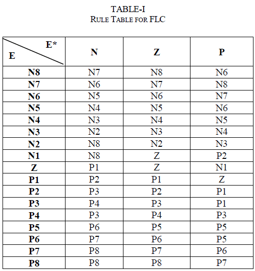
| The membership function values are assigned to the linguistic variables using seventeen fuzzy subsets. Table-I shows the rules of FLC. E and E* are input variables, where E is the error between the reference and actual voltage of the system, E* is the change in error in the sampling interval. |
| B. Inference Engine |
| Mamdani method is used with Max-Min operation fuzzy combination. Fuzzy inference is based on fuzzy rules. Rules are framed in inference engine block. The output membership function of each rule is given by MIN (Minimum) operator and MAX (Maximum) operator. |
| C. Defuzzification |
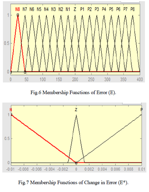
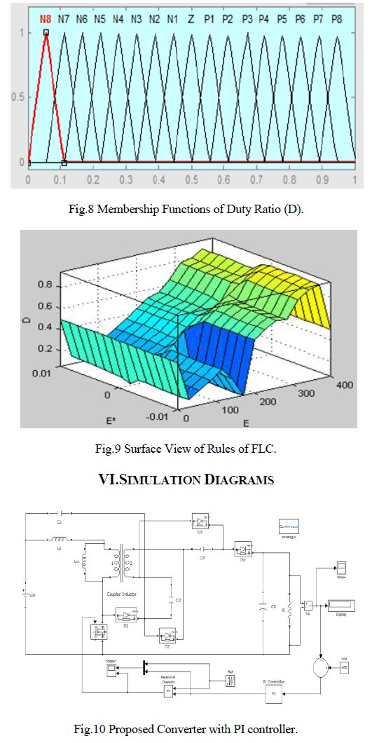
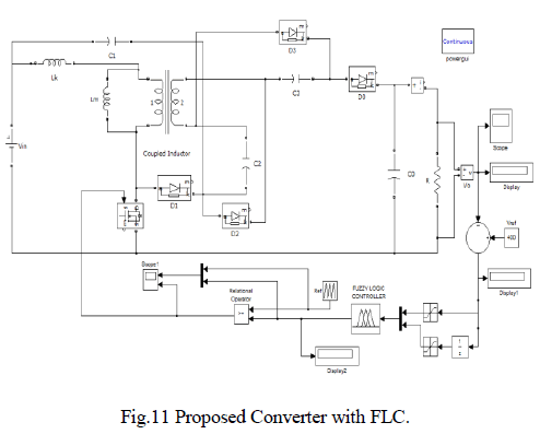
| The output of fuzzy controller is a fuzzy subset. As the actual system requires a non fuzzy value of Control, defuzzication is required. Defuzzifier is used to convert the linguistic fuzzy sets back into actual value. The membership functions of error (E), change in error (E*) and Duty ratio (D) are shown in fig. 6, 7, 8.Fig.9 shows the representation of the typical Rule Surface of fuzzy logic controller. |
 |
 |
 |
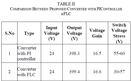
| Fig.10 shows, A24 V input voltage is fed to the converter, an output voltage of 398.3 V is obtained which is fed back as a feedback voltage to the PI controller; there it compares the feedback and the reference signalfromwhichPWM pulse is generated which triggers the main switch of the converter. |
 |
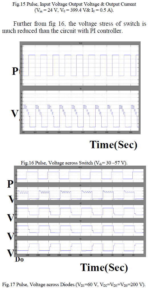
| In fig.11, for the same input voltage the converter is controlled by the newly designed FLC now 399.4 V output voltageis obtained. |
SIMULATION RESULTS |
| A. Simulation Results of Proposed converter with PI controller |
| Fig. 12 shows the response of the converter with PI controller. |
 |
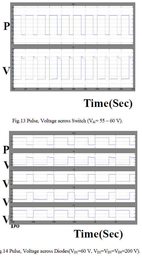
| The switch voltage stress of the converter with PI controller is shown in fig. 13. |
 |
| B. Simulation Results of Proposed Converter with FLC |
| From fig 15, it is clear that for the designed parameters, required output voltage and current is obtained.The duty ratio of the switch is adjusted by FLC to obtain the require output and also the voltage drift problem is eliminated. |
 |
 |
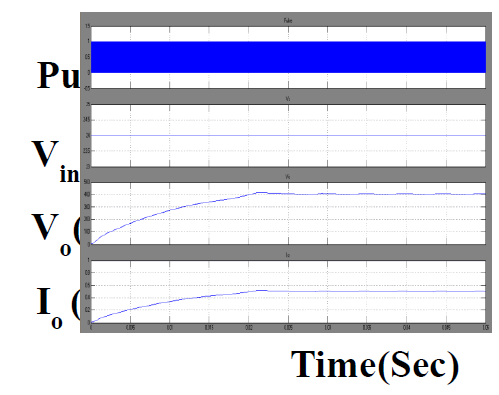
| From fig.17, VD2, VD3, VD0are equal and so, they are under the same voltage ratio, the voltage stresses can be adjusted by the turn ratio of the coupled inductor. |
 |
CONCLUSIONS |
| Here a high step-up dc–dc converter using coupled inductor with fuzzy logic control is simulated. By the capacitor charged in parallel and discharged in series by the coupled inductor, high step-up voltage gain is achieved. As the output voltage of the converter with FLC has minimum overshoot and produces a constant output current shows the better performance compared to the converter with PI controller.These studies could solve many types of problems regardless on stability because as we know that fuzzy logic controller is an intelligent controller to their appliances. Additionally, the switch voltage stress is reduced, thus a switch with low voltage ratings can be selected. |