International Journal of Innovative Research in Science, Engineering and Technology
ISSN ONLINE(2319-8753)PRINT(2347-6710)
ISSN ONLINE(2319-8753)PRINT(2347-6710)
M.Tharangini1*, V.Geetha2 and Dr.G.Murugesan3
|
| Related article at Pubmed, Scholar Google |
Visit for more related articles at International Journal of Innovative Research in Science, Engineering and Technology
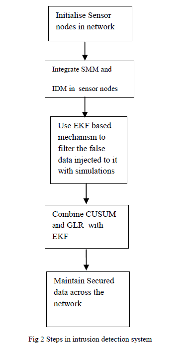
In this paper, a memory efficient new stripe based scanning method for 2- dimensional discrete wavelet transform is proposed in order to achieve an efficient memory and to reduce critical path. The efficient memory is achieved with a stripe based scanning method that enables tradeoff between external memory bandwidth and internal buffer size. Based on the data flow graph of the flipped lifting algorithm, the processing units are developed for maximally utilizing the inherent parallelism. With S number of processing units, the throughput can be scaled while keeping the latency constant. When compared with the existing architecture, the proposed architecture requires less memory. For an N × N image, the proposed architecture consumes only 3N + 24S words of transposition memory, temporal memory, and pipeline registers. The synthesized results in a Modelsim process show that it achieves better area-delay products than the best existing design where S is considered to be 2, 4, and 8.
Index Terms |
| Discrete wavelet transform (DWT), JPEG2000, lifting-based, VLSI architecture. |
INTRODUCTION |
| The discrete wavelet transform (DWT) is being increasingly used for image coding. It is mainly due to the fact that DWT supports superior features like progressive image transmission by quality or by resolution. It is also used in image analysis, video processing, and computer graphics [1]. The DWT is the key component of the JPEG2000 system, and it also has been adopted as the transform coder in MPEG-4 still texture coding. The existing VLSI DWT architectures can be divided into two main categories, namely, convolution-based method and lifting-based method. |
| Compared with the convolution-based methods [2], the lifting-based methods [3] have some favorable characteristics such as fewer arithmetic resources, memory-efficient in-place of less computation, and inherent parallelism [4]. On the other hand, the liftingbased architectures suffer from a long critical path [5]. In order to reduce this critical path various efforts has been made on shortening the critical path delay (CPD) of lifting-based architectures [5]–[12]. The CPDs achieved by these works range between Tm + 5Ta, where Tm and Ta are the delays of multiplier and adder units. Apart from critical path the memory-efficiency advantage of the lifting-based DWT over its convolution based counterpart, since memory requirement is still a major concern in 2-D lifting-based DWT architecture design as it is a size-dominant factor [13]. |
| The memory in 2-D DWT architectures is mainly consisting of temporal memory and transposition memory. Based on different data scanning methods present their memory requirement varies and their impacts on memory sizes can be found in [14] and [15]. A line-based scanning method was used in the structures reported in [7], [9] and [16]. For an N × N image, the best line-based scanning design [11] the total memory required is of 5.5N (words), where 2.5N is used for transposition memory and 3N is used for temporal memory, respectively. Further by introducing a parallel scanning method, Lai et al. [8] and Zhang et al. [10] the transposition memory is reduced to a constant, i.e., 4 and 3, respectively, but requires larger temporal memory of 4N. Several parallel architectures were proposed for lifting-based 2-D DWT [3], [12], [17]. Among the existing 2-D DWT architectures, the design by Mohanty et al. [3] is the best design and achieves the smallest memory of 4N. |
| In this brief, we introduce a new stripe based scanning method which provides efficient memory by reducing the size of line buffer by means of trading external memory bandwidth and internal buffer size. With the newly developed data scanning method, novel memory-efficient parallel 2-D DWT architecture with a short critical path delay of Tm+ Ta is proposed. In [3], Huang et al. introduced a stripe based scanning method for efficient bandwidth-memory tradeoff. The proposed architecture is the most memory-efficient design among the existing ones and requires only 3N + 2S of transposition and temporal memory, with S parallel processing units (PU). The proposed architecture also has constant latency, and its hardware resource requirement and computation time are comparable with those of the best existing designs. The rest of this brief is organized as follows. Section II reviews the lifting scheme and the flipping structure of the DWT, and then, we proposed our modified algorithm for DWT. Section III presents the existing scanning method and architecture for the 2-D DWT. Section IV presents the proposed CSD multiplication and Section V provides performance results and comparisons with previous architectures. Section VI concludes this brief. |
LIFTING METHOD |
| The lifting scheme was first proposed by Daubechies and Sweldens in 1996 [4]. It shows that every finite-impulse response wavelet or filter bank can be factored into a cascade of lifting steps. It means that the polyphase matrices for the wavelet filters can be decomposed into a sequence of alternating upper and lower triangular matrices multiplied by a diagonal normalization matrix. The whole lifting scheme of the 9/7 filter has two lifting steps and one scaling step. In order to minimize the critical path of the lifting-based hardware implementation, a modified algorithm is used by changing the coefficients in lifting formulas [5], shown as follows: |
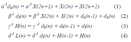 |
| where α, β, γ, and δ are the lifting coefficients, and x(n) is the nth input. Two- dimensional DWT transformation can be achieved with separate row-wise and column-wise 1-D DWT transformation. |
EXISTING ARCHITECTURE |
| A. Stripe based Scanning Method |
| In [17], Stripe based scanning method provides efficient memory by reducing the size of line buffer by means of trading external memory bandwidth and internal buffer size. With the newly developed data scanning method, novel memory-efficient parallel 2-D DWT architecture with a short critical path delay of Tm+ Ta is proposed. In [14], Huang et al. introduced a parallel scanning method for efficient bandwidth-memory tradeoff. However, memory reduction is achieved at the expense of longer computation time. So we introduce a new stripe based scanning method, which has two major differences between the existing scanning methods. The first difference is that the matrix A be an image size Nx(N+1) with one column of zero padded with first column and the next one is that the row-wise DWT is scheduled before the column-wise DWT. Zero padding is nothing but appending zeros to a signal. The structure of stripe based scanning method is shown in Fig 1. |
| The Fig 1(a) shows the image matrix with each small square representing a pixel and the black squares represents the overlapped pixels between two stripes. For S parallel processing units, the stripe width used is 2S + 1, with only one column overlapped between two neighbor stripes. Therefore memory is decreased without increasing the computation time. Row wise operation is performed before column wise operation. During the 1st clock cycle of row wise all the pixels from A(0,0) to A(0,2S) are fed concurrently, where S is the stripe width used. |
 |
| Scanning of an image continues from top down direction from A(N,0) to A(N,2S) where N is the size of image. Alternatively scanning continues from A(0,2S) to A(0,4S) and so on, For N = R × 2S, there are R stripes in total. With our scanning sequence, intermediate matrices H and L are produced by the row processor in the sequence, as shown in the upper part of Fig 1(b) In this the pixels are present in overlapped columns, i.e., A(n, 2rS) for 1 ≤ r ≤ R − 1 and 0 ≤ n ≤ N − 1, a temporal buffer of size N is saved at the expense of reading only one additional pixel for each clock cycle without increasing the computation time. The column processor requires two successive intermediate data from matrix H or L in column order every clock cycle. However, the row processor produces only one pair of intermediate data of H and L per cycle. Thus, intermediate matrices H and L are cached and transposed before being alternatively input to the column processor, as shown in the lower part of Fig 1 (b). Thus the corresponding intermediate H and L are produced. Advantage of this scanning method is that it starts column processing unit as soon as the intermediate results of row processing unit is generated and it is independent of N and S. |
| B. Data processing pipe (DPP) |
| The data flow graph (DFG) of flipping scheme is derived from the equation (1)-(4) where z−1 denotes a unit delay. The basic operation nodes are identical and consist of only addition and multiplication operations. Each node is implemented as a 3-input 2-output Cell, consisting of two adders and a multiplier. The Cell has a CPD of Tm + Ta. We implement the data path in Fig. 2 with the Data processing pipe (DPP) consist of four cells and a constant coefficients α−1, β−1, γ−1, and δ−1, as shown in Fig. 3.It has three inputs namely X0, X1 and X2 along with three partial inputs Pa, Pβ and Pγ and their corresponding partial outputs are produced as Pα’, Pβ’ and Pγ’ and a pair of low and high-pass outputs L and H are produced by scheduling the correct pixel inputs, partial results, and intermediate results of data processing pipe. |
| C. DWT Architecture |
| The pixel inputs and the intermediate pixels obtained through the proposed scanning method, we construct a row processing unit as shown in Fig 3.Since the stripe width is 2S+1,we give 2S+1 pixels are fed concurrently in S DPPs for every clock cycle. For the sth DPP, the three input pixels x0, x1, and x2 are A(n, 2rS + 2s), A(n, 2rS + 2s + 1), and A(n, 2rS + 2s + 2), respectively, and the three |
 |
| corresponding partial outputs as Pα’, Pβ’ and Pγ’ are dh (n, rS + s), dl (n, rS +s), and H (n, rS + s), where 0 ≤ s ≤ S − 1, 0 ≤ r ≤ R − 1, and 0 ≤ n ≤ N −1. Thus, the partial inputs Pa, Pβ and Pγ for the sth |
 |
| DPP are dh (n, rS + s − 1), dl (n, rS + s − 1), and H (n, rS + s − 1). The partial result outputs dh (n, (r + 1) S − 1), dl (n, (r + 1)S − 1), and H (n, (r + 1) S − 1) of the last DPP (s = S − 1) are cached for N cycles to be used by the first DPP for the next stripe. The row processing unit consists of several DPPs. The inputs are fed concurrently to the entire data processing pipe present and their corresponding intermediate results are produced. There is also a presence of temporal memory of size 3N and it is used to store the partial output generated by last DPP and given as an partial input to first DPP thus the intermediate result is produced by row processing unit are fed into transposition register. The basic structure of transposition register is as shown in Fig 4. |
| Each of the row processing unit produces an output of high pass filter as H and low pass filter output as L which is fed into column processing unit through a transposition register. A set of high pass filter output and low pass filter output is passed to the transposition register present so that the output produced is of alternate high and low component. An intermediate H and L are fed alternatively in column processing unit as shown in Fig 5. The partial results produced are consumed by two clock cycles later. At the output of column processing unit four sub bands are produced in an interleaved pattern of (HL, HH), (LL, LH), (HL, HH) and (LL, LH) and so on. The column processing unit starts as soon as the row processing unit output is produced. This architecture reduces the transposition register and size of the temporal buffer used. The output produced by the column processing unit is then scaled. Image scaling is the process of resizing a digital image. |
| Scaling is a non-trivial process that involves a trade-off between efficiency, smoothness and sharpness. The size of an image is reduced or enlarged, the pixels which comprise the image become increasingly visible, making the image appear soft if pixels are averaged, or jagged if not. The scaling coefficient is given as K1 = (αβγδK)2, K2 = (αβγ)2/ K2, and K3 = (αβγ)2δ. Finally the output obtained consist of four sub bands namely HH, LL, HL, LH. Fig 6: shows the overall architecture. For multilevel decomposition, the same DWT core can be used in a folded architecture with an external frame buffer for the LL subband coefficients. |
 |
CSD BASED DESIGN FOR DWT |
| With reference to the existing method [17], the architecture contains more number of multipliers which can be reduced by Canonical signed digit (CSD). It is a multiplier less architecture. Each of the multiplier unit is replaced with shifters and adders for CSD implementation of DWT. The bit-level multiplication of two numbers can be performed by shift and add operation in the simplest form. It has been observed that the complexity of a shiftadd type signed multiplier is depends on the number of one’s of the 2’s complement representation of the multiplicand number with the shifted partial sum whereas the zeros will only shift the partial sum. Canonic signed digit (CSD) are popular for representing a number with fewest number of non-zero digit. No 2 consecutive bits in a CSD number are non-zero. The CSD representation of a number contains the minimum possible number of nonzero bits and it is unique. |
 |
| A. CSD conversion algorithm |
| Let S is the mantissa of multiplier, C is the CSD code and B is the auxiliary carry. The first auxiliary carry is set to 0.Starting from the LSB, scan two bits at a time and CSD code is obtained using the following equations |
 |
| Bi is obtained according to the conventional arithmetic rule. It is equal to 1, when there are 2 or more ones among Bi, Si+1, Si [1]. The CSD code for 7 (0111) is 100-1 |
 |
| B. Multiplication using CSD |
| The CSD multiplication unit contains CSD recoding block, shift control unit, adder unit and twos complement unit. CSD recoding block, converts the given number to CSD representation. Twos complement unit is used to obtain twos complement. Initially, the two operands i.e. multiplier and multiplicand are stored in registers. The mantissa of multiplier is given to CSD recoding unit to obtain CSD code of multiplier. The multiplicand is given to 2s complement unit to get its 2s complement. The multiplicand and its twos complement are given to shift control unit and the partial products are generated by performing required number of shifts based on the sign and position of non-zero digits. The obtained partial products are added in the adder unit. The result is normalized and rounded to get the final product. |
| The block diagram of CSD multiplication is shown in Fig 7. |
 |
PERFOMANCE RESULTS AND COMPARISONS |
| A. Hardware Estimation |
| The hardware utilization of the existing DWT architecture has 3N temporal buffers, 14S pipeline registers, 8S registers for partial results, 2S transposition registers, 10S multipliers, and 16S adders and for the proposed CSD method it can be further reduced. |
| B. Comparison |
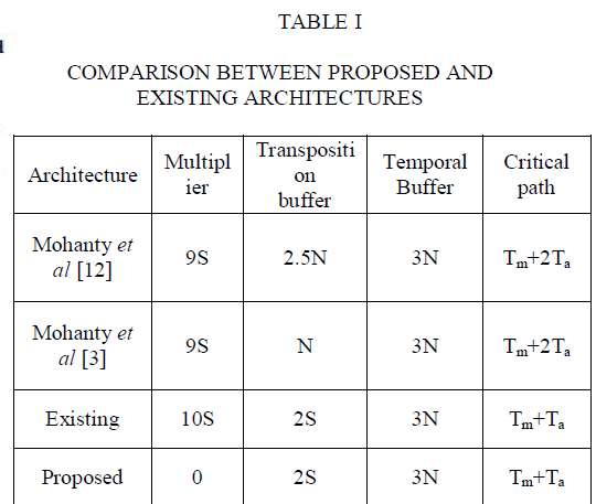
| Table I shows the comparison of the existing architectures and the proposed architecture for 2-D DWT in terms of multipliers, adders, on-chip memory devices, CPD, computation time, and TP. When compared with the existing parallel architectures in[12] and [17], the proposed architecture is multiplierless and critical path is minimized. |
| C. Implementation |
| The proposed design with the different S [S=2, 4, 8] was synthesized using Modelsim and the comparison was done with the existing parallel 2D dwt architectures[3]. The image size of 512x512 is synthesized with 16 bit inputs. |
 |
CONCLUSION |
| In this brief, we have proposed a memoryefficient 2-D parallel DWT architecture with regular structure and short critical path. The efficient memory is achieved by using stripe based scanning method and critical path is reduced to Tm+Ta when compared with [12] B. K. Mohanty, A. Mahajan, and P. K. Meher (2012), where the critical path produced is Tm+2Ta.The proposed method enables the tradeoff between the external input bandwidth and the internal buffer size. Based on the stripe-based scanning method, a new row PU and a new column PU are developed. This architecture achieves the smallest memory size of 3N+24S. |