International Journal of Innovative Research in Science, Engineering and Technology
ISSN ONLINE(2319-8753)PRINT(2347-6710)
ISSN ONLINE(2319-8753)PRINT(2347-6710)
K.Vijaykaran1, Mrs.J.Jeyashanthi2,
|
| Related article at Pubmed, Scholar Google |
Visit for more related articles at International Journal of Innovative Research in Science, Engineering and Technology
The proposed work is to design a positive buck-boost converter with mode-select circuit and with wide range of input voltages. Four switches produce more switching and conduction losses when the converter operates in high frequency. In order to avoid those losses, we employ mode-select circuit in which the converter can work in three different modes as buck, boost and buck-boost mode. With the mode-select circuit the losses in switches are reduced and by the way the converter efficiency is improved. To lessen the loss of switches as the positive buck-boost converter operates in wide range of supply voltages, it is essential to avoid power converters operating in buck-boost mode. By implying feed-forward techniques, the proposed converter can improve its transient response when the supply voltages are changed. It is typically used to compensate for input variations and provide tighter control response of the output voltage. With the above mentioned techniques the proposed converter can get better power efficiency and extends the battery life. The proposed work was simulated by using MATLAB R2012a (v.7.14).
Keywords |
| Mode-Select Circuit, Feed-Forward Techniques, Positive Buck-Boost Converter. |
INTRODUCTION |
| Recently, with the flourishing of portable devices and the development of semiconductor manufacturing technology, conversion efficiency, power consumption and size of devices have become the most important design criteria of switching power converters. Power converters are often applied to LED products, notebooks, mobile phones, and car electronic products. For portable applications, in order to provide consumers better conveniences, how to extend battery life and improve the conversion efficiency of power converters are challenges for designers. Therefore, it is essential to develop accurate switching power converters, which can reduce more wasted power energy [1]. A very common power handling problem, especially for portable applications, powered by batteries such as cellular phones, personal digital assistants (PDAs), wireless and digital subscriber line (DSL) modems, and digital cameras, is the need to provide a regulated non-inverting output voltage from a variable input battery voltage. The battery voltage, when charged or discharged, can be greater than, equal to, or less than the output voltage. But for such small-scale applications, it is very important to regulate the output voltage of the converter with high precision and performance. Thus, a trade-off among cost, efficiency, and output transients should be considered [6]. A common power handling issue for space-restrained applications powered by batteries is the regulation of the output voltage in the midrange of a variable input battery voltage [11]. There are various topologies such as inverting buck-boost converters, singleended primary inductance converters (SEPICs), Cuk converters, isolated buck-boost converters and cascaded buck and boost converters, which can be implemented to maintain a constant output voltage from a variable input voltage. |
| The important points of concern for such low-voltagerange power supplies are output ripple, efficiency, space and the cost. The above mentioned topologies are generally not implemented for such power supplies due to their lower efficiency, higher size and cost factors. The most difficult problem is the spikes in the output voltage, which causes the converter to lose efficiency during the transition from buck mode to the boost mode. Cost, size, switching speed, efficiency and flexibility all need to be considered in designing such power supplies. The advantage of having higher efficiency is longer runtime at a given brightness level from the same set of batteries. With increasing low-voltage portable devices and growing requirements of functionalities embedded into devices, efficient power management techniques are required to extend battery life. In order to effectively use the remaining capacity of the battery, the design of dc-dc converters need to supply the portable devices a regulated voltage over a wide battery voltage. The limitations of standard analog pulse width modulator (PWM) causes uncontrolled pulse skipping and significantly increased output voltage ripples when the converter operates in the transition region of the buck and boost modes. |
 |
| That is, a buffer region, which is buck-boost mode, is required to provide a smooth and stable transition between two modes. The converter can operate in buck, buck-boost and boost modes when the battery voltage decreases. Since the dc-dc converter has different operation modes, the system stability, the output ripple, and the accuracy of the regulated output voltage during mode transition need to be guaranteed [3]. |
PROPOSED METHOD |
 |
| In this proposed work, the positive buck-boost converter can operate in buck, boost, and buck-boost mode. The highest ratio occurs in buck-boost mode; the positive buck-boost converter causes switching loss and conduction loss because of its four power transistors. To reduce the loss of switches, as the positive buck-boost converter operates in wide-range of supply voltages, it is necessary to avoid power converters operating in buckboost mode. Therefore, we design a mode-select circuit to detect the battery energy and select the operation mode [1]. When the converter operates in buck mode or boost mode, it only switches two power transistors. The mode-select circuit can reduce the conduction loss and switching loss of the proposed converter, and the power efficiency can be improved. The proposed converter can operate in wide supply voltage range and extend the battery life. |
| A. Mode-Select Circuit |
| The use of four power transistors produces more switching losses and conduction losses when operated in high frequency. To avoid those losses we utilize mode-select circuit and we can operate in three different modes as buck, boost and buck-boost mode. The mode-select circuit can avoid overlapping of the modes; it can decide the mode to operate when needed. Then it can avoid turning on the power transistors at the same time. Finally, it can determine the operation mode by a control signal from controller. By using this we can extend the battery life and operate the converter in efficient way. |
| B. Modes of Operation |
| Fig.3 (a) shows the proposed converter operating in the charging interval of buck mode; the power transistors S1 and S2 are turned ON and the power transistors S3 and S4 are turned OFF. Fig.3 (b) shows the proposed converter operating in the discharging interval of buck mode; the power transistors S2 and S3 are turned ON and the power transistors S1 and S4 are turned OFF. Fig.4 (a) shows the proposed converter operating in the charging interval of boost mode; the power transistors S1 and S4 are turned ON and the power transistors S2 and S3 are turned OFF. Fig.4 (b) shows the proposed converter operating in the discharging interval of boost mode; the power transistors S1 and S2 are turned ON and the power transistors S3 and S4 are turned OFF. Fig.5 (a) shows the proposed converter operating in the charging interval of buck-boost mode; the transistors S1 and S4 are turned ON and the power transistors S2 and S3 are turned OFF. Fig.5 (b) shows the proposed converter operating in discharging interval of buck-boost mode; the power transistors S2 and S3 are turned ON and the power transistors S1 and S4 are turned OFF. |
 |
 |
| Fig.5 (a) Charging interval of buck-boost mode. (b) Discharging interval of buck-boost mode. |
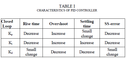
| C. PID Controller |
| By employing PID controller the converter operates effectively and improves the output voltage, when the supply voltage changes. It gives better performance than PI controller, by reducing rise time and increasing gain value the converter responds faster to changes in set point value. |
| The PID controller parameter are Kp = 4.5, Ki = 0.01and Kd = 0.001. It reduces the steady state error by compared it with set point voltages for different modes of operation. |
 |
SIMULATION RESULTS |
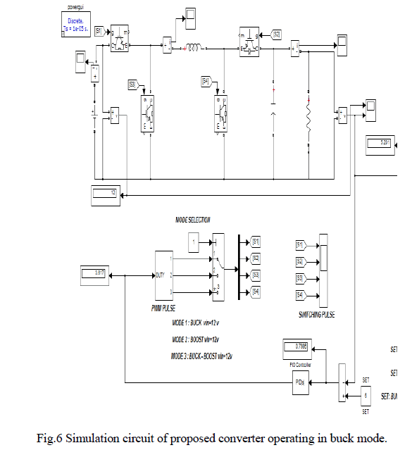
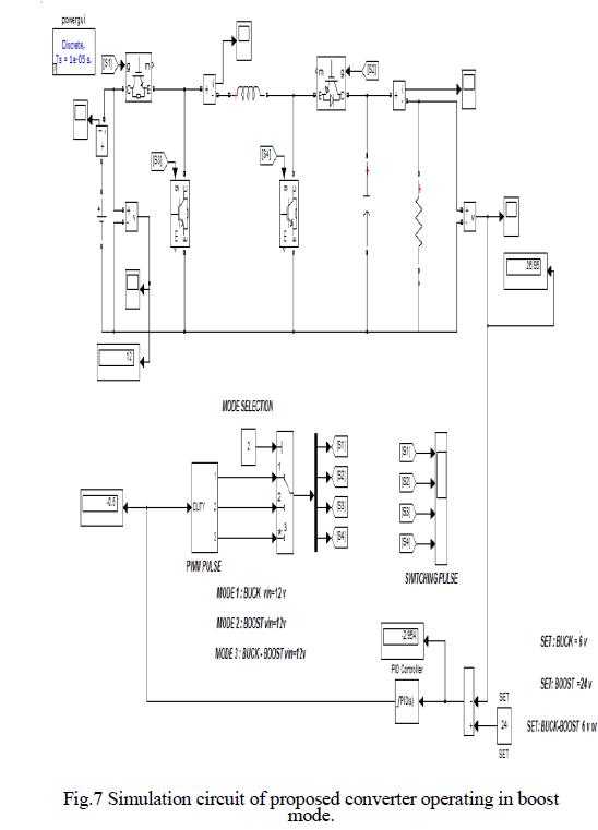
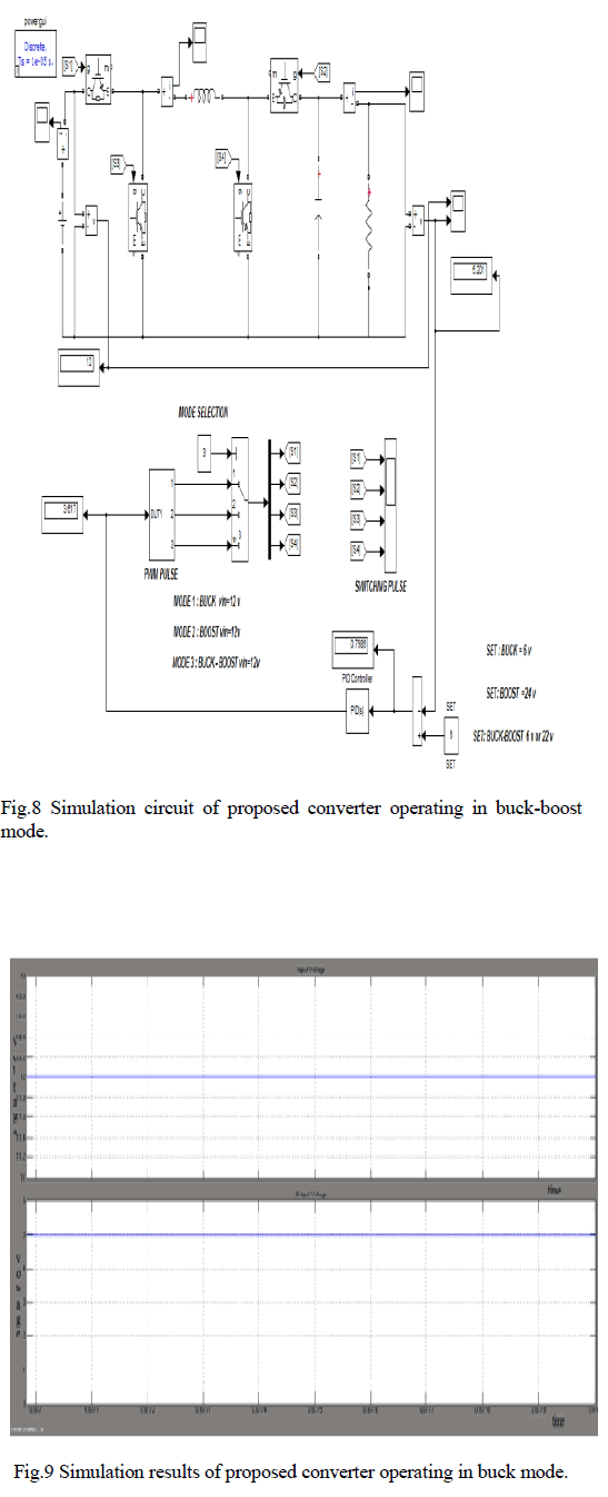
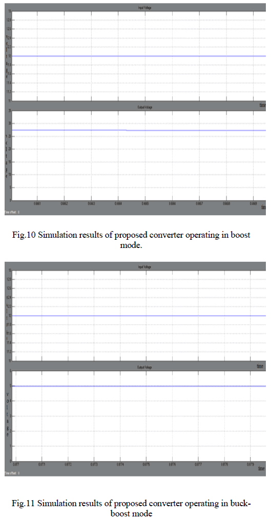
| A Positive buck-boost dc-dc converter with mode-select circuit using PID controller has been simulated and results were obtained. The output voltage is different for all the three modes as 6v for buck mode, 24v for boost mode and either 6v or 24v for buck-boost mode. Fig.6. shows the simulation circuit of proposed converter operating in buck mode. Fig.7. shows the simulation circuit of proposed converter operating in boost mode. Fig.8. shows the simulation circuit of proposed converter operating in buckboost mode. Fig.9. shows the simulation results of buck mode; supply voltage = 12v, output voltage = 6v. Fig.10. shows the simulation results of boost mode; supply voltage = 12v, output voltage = 24v. Fig.11. shows the simulation results of buck-boost mode; supply voltage = 12v, output voltage = 6v. |
 |
 |
 |
 |
CONCLUSION |
| Thus the implementation of a positive buckboost converter with mode-select circuit and with wide range of input voltages is proposed in this paper. Four power transistors produce more conduction losses and switching losses when operated in high frequency. To avoid those losses in switches we employ mode-select circuit. By using mode-select circuit we can operate the converter in three different modes as buck, boost and buck-boost mode. By this we can minimize the losses in switches and operate the converter in efficient way. To minimize the loss of switches, as the positive buck-boost converter operates in wide range of input voltages, it is necessary to avoid power converters operating in buckboost mode. Therefore, we design mode-select circuit to detect battery energy and select the operating mode. Using feed-forward techniques, the proposed converter can improve its transient response when the supply voltage changes. It is typically used to compensate the input variations and provide tighter control response of the output voltage. By using the above mentioned techniques, the proposed converter improves power efficiency and extends the battery life. |
References |
|