International Journal of Innovative Research in Science, Engineering and Technology
ISSN ONLINE(2319-8753)PRINT(2347-6710)
ISSN ONLINE(2319-8753)PRINT(2347-6710)
| Benjamin. J1, Grace Jency. J1, Vijila. G1 Department of ECE, Karunya University, Karunya Nagar, Coimbatore – 641114, India |
| Related article at Pubmed, Scholar Google |
Visit for more related articles at International Journal of Innovative Research in Science, Engineering and Technology
The concept of miniaturization was introduced because of advancement in science and technology during 1980s. These miniaturized structures and designs are of high significance for making up with the macroscopic technology, for the sake of interfacing with microscopic world. The fabrication of micro structures and designs which are the advanced applications of micro fabrication are used for the process of micromachining structures in three dimensions as it is essential for interfacing with the nanotechnology. Micromachining which means performing cutting or grinding operations or selective removal of wafer to produce various structures has much important applications like accelerometers which are used to trigger air bags in cars. The lithography and etching processes are used to shape the bulk materials into microstructures in micro fabrication mechanism. Different ion bombardment techniques and chemical reactive mechanisms are used for a type of etching which is carried out in vacuum chamber, whereas chemical solutions are used for another type of etching mechanism whose procedures are finished in a bath. This survey illustrates different etching methodologies and the impact of various etchants in wet etching.
Keywords |
| Etching, orientation of crystal, etchant, TMAH, KOH, EDP, concentration of etchant, temperatureof etchant |
INTRODUCTION |
| There are a lot of processing steps in the process of micro fabrication. Etching is an important step in the process of micro fabrication. The term etching refers to the removal of layers from the surface of wafer when manufacturing. This is a critically important process, each and every wafer undergo a lot of etching process. The material which is used to protect the wafer from the etchants is known as the masking material, which is used in many etching steps to resist etching. This masking material can be a photoresist and it is patterned using photolithography.Etching can also be referred as making cavities and these cavities should have specific depth according to the purposes. The depth of such cavities produced can be controlled by etching time and the etching rate. The success in performing etching mechanism is that, the top layer of a multilayer structure should be removed entirely, without any kind of damage in the underlying layers or the masking layers. This entirely depends on the ratio of the etch rates of two materials which is termed as selectivity. During some cases of etching, etches undercut the mask layer and it produces sloping sidewalls forming cavities. The distance of undercutting is called bias. |
TYPES OF ETCHING |
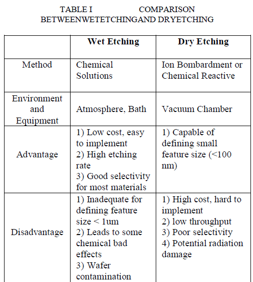
| Fundamental etching techniques used in micro fabrication are dry etching (plasma phase) and wet etching (liquid phase). The disadvantages of dry etching are as follows, the gases used in dry etching are quite toxic and corrosive. It requires redeposition of nonvolatile compounds and it needs specialized and expensive equipment. |
 |
| Wet etching is inexpensive and it has been extensively used for the fabrication of MEMS components such as diaphragms based on single crystal silicon, especially on (100) water and cantilever beam.Wet etching is the process of removing a material by using liquid chemicals or etchants from a wafer. The specific patterns are defined by masks on the wafer. Materials that are not protected by the masks are etched away by liquid chemicals. These masks are deposited and patterned on the wafers using lithography. Wet etching process involves multiple chemical reactions that consume the original reactants and produce new reactants. |
 |
 |
| A. ISOTROPIC ETCHING |
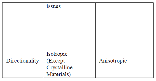
| Wet etchants are often isotropic and they lead to larger bias during the etching of thick films. They also require disposal of large amounts of toxic waste. This etch method is particularly effective just before "backend" processing (BEOL), where wafers are normally very thin after wafer backgrinding and are very sensitive to thermal or mechanical kind of stress. Etching a much thin layer of few micrometers will remove micro cracks produced during back grinding resulting in the wafer having dramatically increased strength and flexibility. This type of etching is quick, easy and cheap. Rounding of sharp anisotropic corners is used to avoid stress concentration. This exhibits same etch rate in all directions. Lateral etch rate is about as same as the vertical etch rate. This etch rate never depends on the orientation of the mask edge. For isotropic wet etching, a mixture of hydrofluoric acid, nitric acid, and acetic acid (HNA) is the most common etchant solvent for silicon [1]. The concentrations of each etchant determines the etch rate. Silicon dioxide or silicon nitride is often used as a masking material against HNA. When the reaction occurs, material is removed laterally at a rate similar to the speed of downward etching. Wet chemical etching is generally isotropic even though a mask is present since the liquid etchant can penetrate underneath the mask. If the directionality isof much importance for high-resolution pattern transfer, process of wet chemical etching is normally prohibited [1,2]. |
 ' ' |
| B.ANISOTROPIC WET ETCHING |
| This is also known as Orientation Dependent Etching. Liquid etchants etch crystalline materials at different rates depending upon which crystal face is exposed to etchant used. A large difference in the etch rate is there depending on the silicon crystalline plane. When silicon like materials are used, this effect can allow very high anisotropy. The key technique for the fabrication of various micromechanical devices is anisotropic etching. The etch rate (ER) in anisotropic etching is much faster in etching plane as etch time progress usually the (111) planes of silicon. The important factor of anisotropy etching includes selectivity, handling and process compatibility and anisotropic. Anisotropic wet etching produces a typical etch rate about 1μm/min. |
 |
FACTORS AFFECTING ETCHING |
| A. BASED ONTHE ORIENTATION OF CRYSTAL |
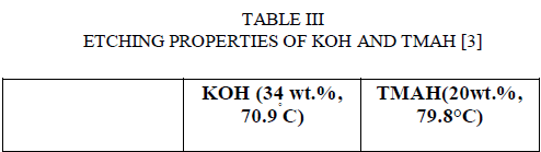
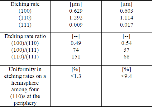
| The orientation of the crystals is one of the prime factors that affect etching. There are a lot of cases where the mechanism of etching gets affected because of the crystal orientations.The concept of Miller Indices is very important for this study about the orientation of crystal as it is used to specify the directions and planes. These directions and planes could be in lattices or in crystals. The number of indices will match with the dimension of the lattice or the crystal. The importance of the miller indices is that, in Materials Science it is important to have a notation system for atomic planes since these planes influence the Optical properties, reactivity of material, Surface tension and dislocations.The etch rates differ for different crystal orientations which are known to us by the concept of miller indices. |
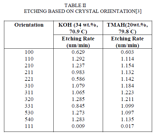 |
| The hillocks [4-8] were bounded by (111) crystal planes. The dependences of the (110) etch rates shows a similar tendency to those of the (100) plane. The etch rates are higher than those for the (100) plane. As the concentration increases, the smoothness of the etched (100) surface changed. Etching of silicon(110) surface revealed that at 10 wt %, the surface was covered by an irregular pattern and a ridged pattern in the <110> direction. |
B.BASED ON THE TYPE OF ETCHANT |
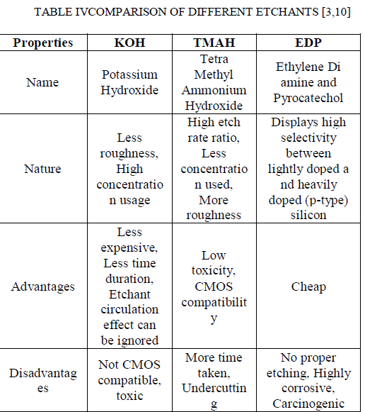
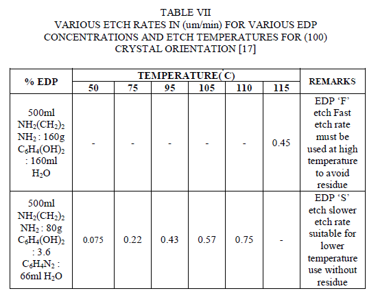
| The etchant EDP stands for Ethylene diamine - Pyrocatechol. EDP etching is readily masked by SiO2, Si3N4, Au, Cr, Ag, Cu and Ta, but EDP can etch aluminum. This etchant is very corrosive, carcinogenic and it does not etch as much as KOH does.This etchant will rust any metal in the nearby vicinity. It leaves brown stains on surfaces that are difficult to remove.EDP has a faster etch rate on convex corners than other anisotropic etches. It is generally preferred for undercutting cantilevers. Just because the rapid etching process of convex corners exhibits a polishing action,it usually tends to leave a smoother finish than other etches. Even though this etchant has so many advantages, it is completely incompatible with MOS or CMOS processing. So this etchant is not used widely and the usage of this etchant has been reduced significantly for the process of anisotropic etching. |
| TMAH stands for Tetra Methyl Ammonium Hydroxide, which has more advantages of all etchants used. This etchant exhibits low toxicity and CMOS compatibility [9]. Even though the processing time period is high for etching using TMAH than using KOH, usage of TMAH gives us the best etched surfaces than the etched surfaces got from KOH. Perfect wafer squares are got at less time when KOH is used than that of TMAH because of etch rates for all the crystal orientations. Even though the processing time is less for process involving KOH, they do not provide the etched perfect wafer squares. But the advantage of TMAH is that, even though it requires more processing time periods, the etched wafer squares will be perfect. The important properties of anisotropic silicon etchants are anisotropy [8], selectivity, handling and process compatibility. The process compatibility becomes especially important, since sensors and actuators need to be utilized within circuits on the same chip to realize a new transducer system with high performance. Tetramethyl ammonium hydroxide (TMAH, (CH3)4NOH) [10] solutions with various concentrations from 5 to 40 wt % and temperatures can be used for wet anisotropic etching purpose. The main feature of TMAH is its compatibility, since it has been utilized in the etching process as the developing solution of positive photoresist. Thusthe semiconductor-grade solutions can be obtained. |
 |
 |
| The etchant KOH (Potassium Hydroxide) is used as an alternative for EPD etchant and it is the most used of all hydroxide etches. Presence of alkali metal (potassium, K) makes this completely incompatible with MOS or CMOS processing. It is comparatively safe and non-toxic than KOH. Usage of KOH, introduces the mobile potassium ions into the wafer thereby making the wafer toxic. When this etchant is used, the etch rate increases along with the processing time period. |
 |
 |
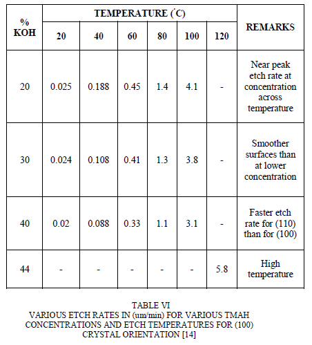
| TABLE V VARIOUS ETCH RATES IN (um/min) FOR VARIOUS KOH CONCENTRATIONS AND ETCH TEMPERATURES FOR (100) CRYSTAL ORIENTATION [11] |
C. BASED ON THE TEMPERATURE AND THE CONCENTRATION OF ETCHANT |
| In case of KOH, The optimum temperature at which the etching process is carried out using this etchant is 80Ãâ¹ÃÅ¡C and the etchant concentration taken for this condition is 35%. This is because the optimum etching rate with minimum surface roughness is obtained in this condition [12]. The etch rate is inversely proportional to the etchant concentration and is directly proportional to the temperature. For this optimum amount of etchant concentration, the galvanic etch stop worked much better by producing the membranes with equal amount of thickness of about 6um, but when the etchant concentration is less, still then the galvanic etch stop functioned, but then the membranes produced were slightly more thicker of about 10 um. 22 wt. % KOH solution provides maximum silicon etch rates of 89.2 and 88.1 μm/h for n-type and p-type silicon respectively at 80 °C [1]. The dopant type of silicon substrate has little effect on the etch rate of silicon although n-type etches slightly faster than p-type silicon. The silicondioxide etch rate increases continuously with increase in temperature irrespective of KOH solution concentration. The maximum silicon dioxide etch rate is 450 nm/h at 80°C using 33 wt. % KOH. The Al etch rate is appreciable in all KOH concentrations with maximum etch rate of 3.0 μm/min. The etched silicon surface smoothens with both increase in KOH concentration and bath temperature [13]. Silicon surface roughness degrades with increase in etch duration due to the masking of hydrogen bubbles evolved during etching which significantly contributes to surface roughness. |
 |
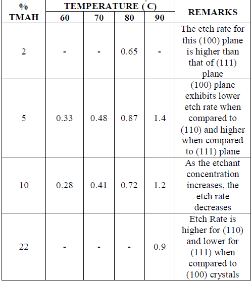
| Using pure TMAH will lead to severe undercutting and so 25% of TMAH is used for etching process. The etching process using this etchant is carried out at 90Ãâ¹ÃÅ¡C temperature [15]. This is because, the best range of temperature for this process is 70Ãâ¹ÃÅ¡C – 90Ãâ¹ÃÅ¡C, but the optimum etching rate is obtained only at the highest value of temperature in this specified range. The etchant concentration is taken as 25% as pure TMAH causes high undercutting [9]. The other specific reason for usage of 25% concentration is because the surface roughness decreases with increase in the TMAH concentration and the smooth surfaces are obtained only with 25% TMAH. Even here, the etch rate decreases with increase of etchant concentration and the etch rate increases along with temperature. |
| Usage of concentration of etchant in the case of TMAH (25%) is less when compared to the usage of concentration in the case of KOH (35%), but at the cost of increased processing time. The dependences of the etch rates of (100), (110) and (111) crystal planes on temperature and concentration, the selectivity to SIO2 and S13N4 , the dependence of aluminum etch rates on the amount of dissolved silicon, the dependences of polysilicon etch rate on boron concentration and the electrochemical etching characteristics can also be evaluated. Experiments shows that etch rates decrease with increasing concentration. At 5 wt %, the etched surface was sometimes covered with pyramidal hillocks and the etch rate became very low. As the concentration increases, the smoothness of the etched (100) surface changed drastically. At 5 wt %, the surface was covered with pyramidal hillocks having high densities. With an increase in concentration from 5 to 15 wt %, the density of the hillocks decreased and smaller hillocks were obtained. Above 22 wt %, a very smooth surface was obtained. The measured roughness for the 22 wt % solution was within 100 nm. There is no significant dependence of roughness on temperature. With an increase in concentration from 5 to 22 wt %, the roughness became smaller and rather a smooth surface was obtained at 30 wt%. The aluminium [16] etch rate shows that an increase in the amount of dissolved silicon, the aluminium etch rate decreased. At more than 40 g/l dissolved silicon, the aluminium etch rate decreased rapidly. An aluminium etch rate of 0.01 was obtained for 67 g/l of dissolved silicon. |
 |
CONCLUSIONS |
| The etchants used for etching process are clearly discussed about along with the advantages and disadvantages of the etchants in correspondence to their respective etchant concentration and temperature at which the etching process is carried out. The wafer squares which undergo etching because of the etchants used must get the perfect wafer squares after the compensation structures get etched off. That condition gives us the clear idea of the processing time at which the perfect etch square is obtained.Some of the etchants which aresubjected surfactants and non-ionic to KOH and TMAH solutions, were used to evaluate the etching properties under various operating parameters including the etching rate and roughness quality of the (100) silicon plane, the selectivity of silicon dissolution toward silicon dioxide and reduction of the undercutting at convex corners.The etch rates of (100) and (110) decrease with increasing concentration. As the concentration increases, the roughness of the etched surface is reduced and a very smooth surface is obtained.The etch rates of aluminium were reduced by dissolving silicon in TMAH solution. It was confirmed that the etch-stop techniques using a heavily borondoped layer or p-n junction were applicable to TMAH solutions. It can be concluded that TMAH is a promising solution for silicon micromachining as one of the useful etchants having good compatibility. In the case of surfactant added TMAH, it is difficult to make sharp edge convex corners using the corner compensation method. |
References |
|