International Journal of Innovative Research in Science, Engineering and Technology
ISSN ONLINE(2319-8753)PRINT(2347-6710)
ISSN ONLINE(2319-8753)PRINT(2347-6710)
VIDHYASHREE H K1 and THIPPESWAMY K H2
|
| Related article at Pubmed, Scholar Google |
Visit for more related articles at International Journal of Innovative Research in Science, Engineering and Technology
This paper presents how power is reduced using voltage scaling method. By scaling the voltage down the power will be reduced but the low voltage increases the parametric failures like access, disturb and write. In this paper propose SRAM cell architecture with the application of low voltage for Lower ordered bits & nominal voltage for Higher ordered bits, because for multimedia applications like image, vidéo and audio has inherent error tolerance. The proposed SRAM cell architecture is constructed using 45nm technology(transistor size, with Gate Length is 45nm ).Simulations results is shown how power is reduced for proposed SRAM cell architecture in comparison with standard SRAM cell. Along with power reduction the proposed SRAM cell architecture is tested under process and temperature variations.
Keywords |
| Voltage scaling, Low-power, SRAM cell, Process variation, Temperature variation, Multimedia applications. |
INTRODUCTION |
| In order to improve the energy efficiency of mobile multimedia systems performing image, video and audio processing applications we have to reduce the memory power[1][2]. By scaling the voltage down the power will be reduced but the low voltage increses the parametric failures like access, disturb and write in sram array due to manufacturing and intrinsic device variations[3].With voltage scaling the data in the memory leads to higher bit error rate and limiting the advantage of voltage scaling and hence power saving.But multimedia applications like video and image has inherent error tolerance and provide acceptable QOS(Quality Of Service) even with non_negligible amount of bit error rate.with this error tolerance quality voltage scaling can be performed in SRAM array for multimedia and communication applications [4], [5]. By scaling the voltage in all the bits of pixels wiht same voltage increases error rates in all the bits and leads to faster degradation of quality of image.the lower significant bits of an image pixel and many other signals like audio, vedio are more tolerant to noise than higer significant bits in multimedia applications. Hence power saving can be done with less image quality degradation dy appling low voltage for lower significant bits and high voltage for higher significant bits[6]. |
| The sram array in a mobile system will be shared by diffrent applications with varing error tolerance but data centric applications do not have this quality.For different kinds of image there will be different error tolerance ability and hence, SRAM array need to support dynamic reconfiguration of number of bits in the low-voltage mode.there will be diffrent quality of degradation for different images or applications.The supply voltage,wordline and bitline voltage of an SRAM cell will also be responsible for diffrent failure mechanisms.hence, proper configuration of diffrent voltage levels is necessary to dynamically modify in the low voltage and high voltage modes.Which is not achieved in standard SRAM VLSI μ-architecture [8]. |
LITERATURE SURVEY |
| By referring to [1] it propose the effort to analyze the power and performance of realistic motion estimation algorithms in both hardware and software realizations. For custom hardware realizations, this paper presents a general model of VLSI motion estimation architectures. Reference [2] presents a compiler-directed scheme to minimize the number of instructions to be generated to manipulate address registers found in DSP architectures. Reference [6] show that probabilistic arithmetic can be used to compute the fft in an extremely energy-efficient manner, yielding energy savings of over 5.6X in the context of the widely used synthetic aperture radar (sar) application . Our results are derived using novel probabilistic cmos (pcmos) technology, characterized and applied in the past to realize ultra-efficient architectures for probabilistic applications.By referring to [7] shows with the emerging SoC era the on-chip embedded memory will occupy most of the silicon real estate. As the technology proceeds into very deep submicron, the yield of SoCs will drop sharply mainly because of the on-chip memory failure. Therefore, the embedded memory is becoming the crucial part for achieving higher chip yield. In this paper, we propose an error resilient video data memory system architecture design. The proposed scheme employs partial memory protection scheme rather than traditional whole memory protection. Our approach is based on the fact that video data memory need not to be error-free because multimedia data has built-in redundancies by their own nature and allows partial data loss without serious quality degradation. With our approach we can achieve 100% data memory yield while incurring a small power overhead. We demonstrate the efficiency of our approach with H.264 application up to 2.0% memory bit error. |
METHODOLOGY |
| The SRAM cell is implemented with the array of 8x8.Along with precharge circuitry to precharge BL and BLBAR lines. And sense amplifier to read the data. |
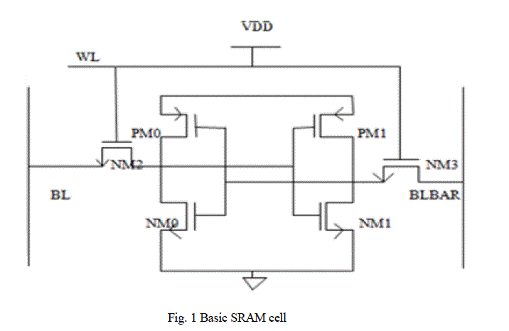
| 1. Basic SRAM cell |
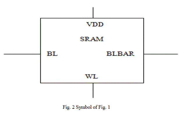
| The schematic of basic SRAM cell with two inverters connected back to back is shown in the Fig. 1. The back to back inverter is a bi-stable flip-flop with two access transistor. The nmos NM0 and NM1 are drive transistor, NM1 and NM2 are access transistors. The pmos PM0 and PM1 are load transistors. The gate of access transistors are connected to the wordline(WL) and the source or drain of access transistors are connected to bitlines(BL).The data is written into the SRAM cell using write circuitry through BL and BL_B into the flip-flop in the write operation and the data is read through sense amplifier in read operation.The corresponding symbol is shown in Fig.2. |
 |
 |
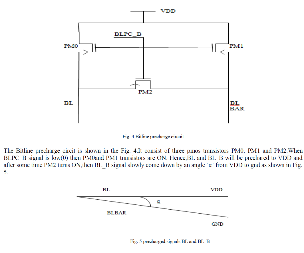
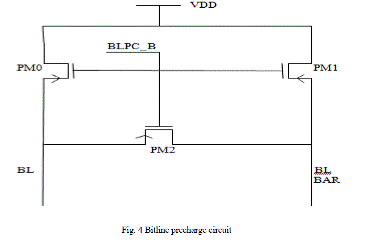
| 3. Bitline precharge circuitry |
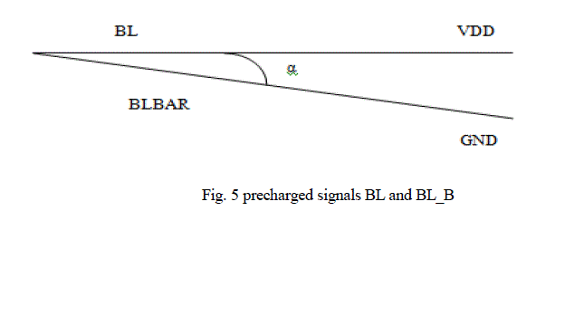
| The Bitline precharge circit is shown in the Fig. 4.It consist of three pmos transistors PM0, PM1 and PM2.When BLPC_B signal is low(0) then PM0and PM1 transistors are ON. Hence,BL and BL_B will be prechared to VDD and after some time PM2 turns ON,then BL_B signal slowly degrades by an angle „α‟ from VDD to „0‟ as shown in Fig. 5. |
 |
| 4. Sense Amplifier with D-Latch |
| The Sense amplifier is the main circuit in the SRAM read operation in order to detect the data in the SRAM cell and is shown in Fig. 6. The sense amplifier shown in Fig. 6 is a Latch type sense amplifier and SAEN signal act as a clock. When SAEN signal is „1‟ the amplifier detects the signal and while „0‟ SAEN_B signal is enabled and hence data will not be detected. D-Latch is used to pass the signal detected. SAEN is given to the clock of D-Latch and SAEN_B is given to the the clockbar of D-Latch. The schematic representation of D-Latch is shown in the Fig. 7. |
 |
PROPOSED ARCHITECTURE |
| The standard 6T SRAM cell is shown in the Fig. 1. Which is basically used to store the data this is compared with proposed architecture how power is reduced by applying low voltage for lower order bits and nominal voltage for higher order bits, using switching transistors. The proposed SRAM architecture is implemented for write and read respectively. |
| 1. Proposed architecture for write operation |
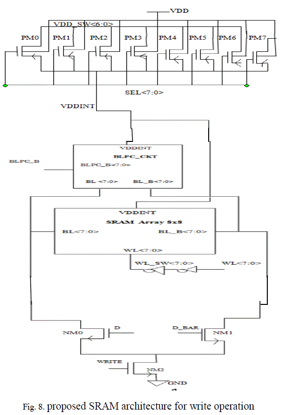
| The proposed SRAM architecture for write operation is shown in the Fig. 8. SRAM Array 8x8 which consist of 8 cells is used to store 8 bits of data. In this architecture we use PMOS (PM0 – PM7) which acts as a switch. when select line which is connected to gate of PMOS is zero the pmos will be on and power supply will be connected to that bitcell. So, higher order bits is applied to nominal voltage and lower order bits is applied with low voltage. Through the signal VDD_SW<6:0>. The power consumption for lower oder bits will be reduced. In write circuitry data is written into the bitcells of SRAM array 8x8 is through three NMOS transistors (NM0 – NM1). The input data will be D, D_BAR & WRITE. Where D and D_BAR are data signal and WRITE is control signal. The BL and BL_B signals of each bitcell of SRAM array 8x8 is precharged through bitline precharge circuitry as shown in Fig. 4. |
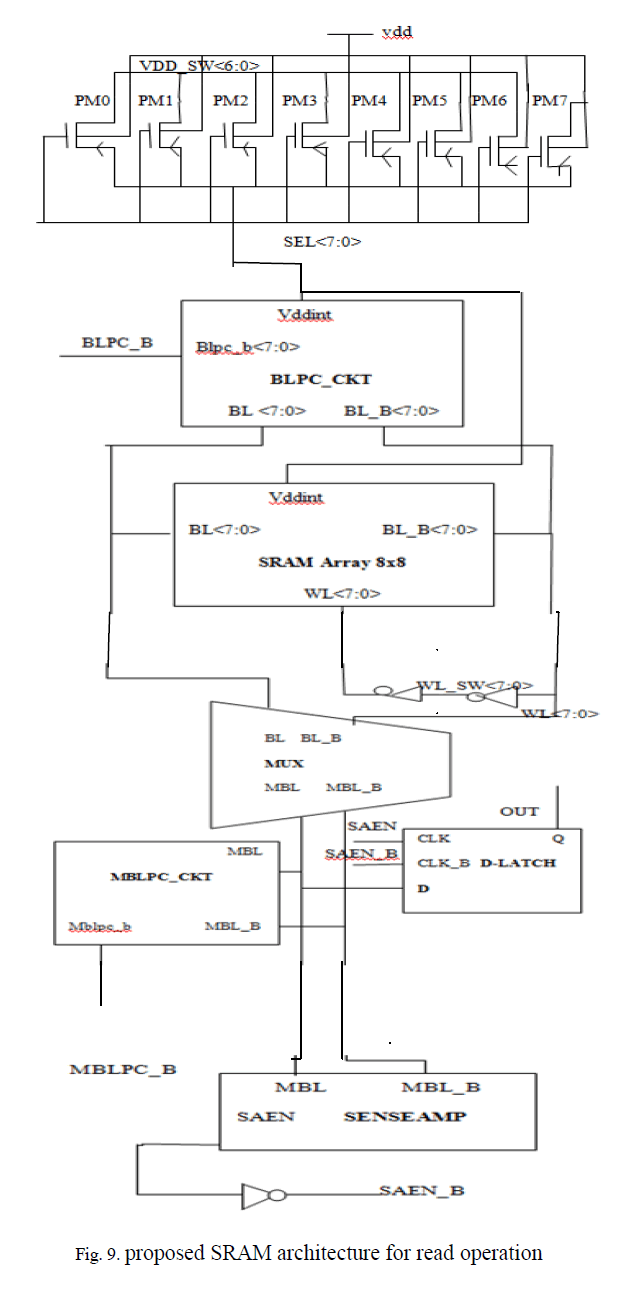
| 2. Proposed architecture for read operation |
| The proposed SRAM architecture for read operation is shown in the Fig. 9. The power supply switching activity to the SRAM Array8x8 is same as given in write operation. The bitlines of each cells of SRAM Array 8x8 is precharged by bitline precharge circuit(BLPC_CKT). In read operation data is sensed by the sense amplifier along with D-Latch circuit. The MUX used is the line to line MUX. To pass the sigmal from SRAM Array 8x8 to Sense Amplifier and MBLPC_CKT. The MBLPC_CKT is required for precharging the bitlines of the selected cell of the array. The sense Amplifier detects the data or the selected cell when enabled by the SAEN signal. |
| Normally in basic SRAM cell only single power supply (constant) value is applied. Where as in proposed architecture switching power supplies with eight transistors applied with eight different voltages that is low voltage for lower order bits and high voltage for higher order bits. So, the part of the power required for lower order bits in the image pixels which is applied with low voltage can be saved in comparison with standard SRAM Array. |
 |
 |
SIMULATION RESULTS |
| The proposed architecture is tested by applying different voltages for different bits of data the result is verified and tabulated . |
| 1. Result of proposed SRAM architecture for write operation |
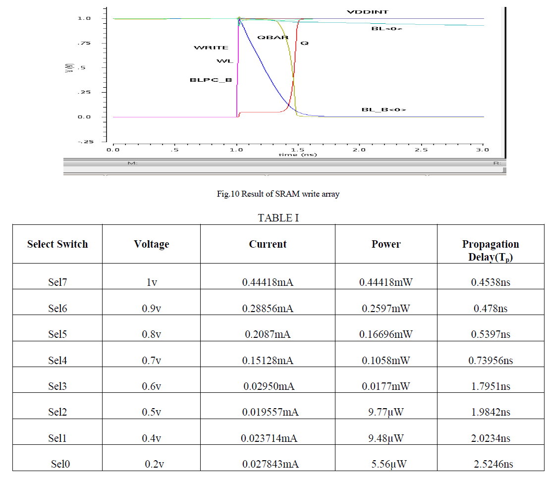
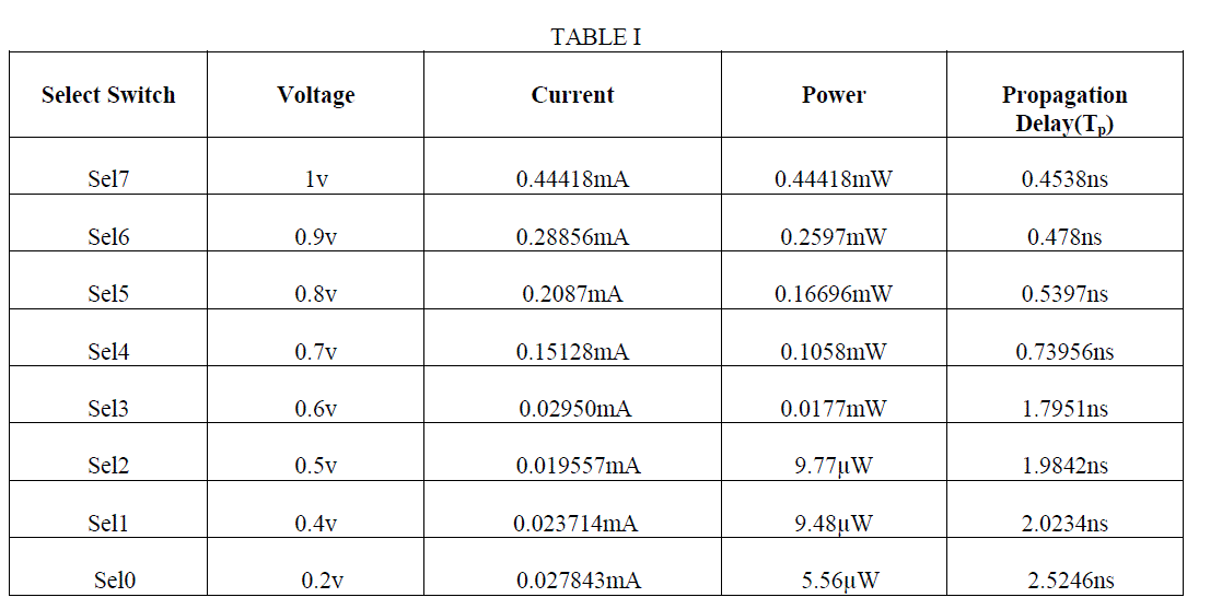
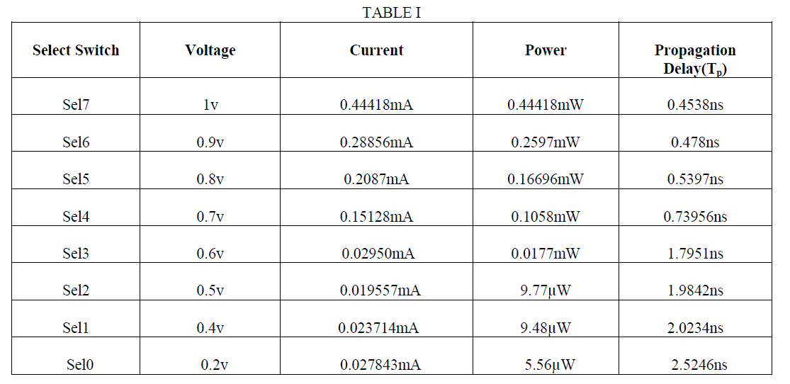
| The output results is shown in the Fig. 10. And table is tabulated in TABLE1. As shown in the Fig.10 the input signals WRITE, WL, BLPC_B is given with the same values. The BL<0> is precharged to VDD and BL_B<0> signal after sometimes comes down to the level GND. Q and Q_BAR signals are the data of SRAM bitcell, from which propogation delay can be found. TABLE I shows the values voltage, current, propagation delay and power for different values of switching supply voltage with different select lines. As the voltage scale down power reduces and propogation delay increases this is the tradeoff. |
 |
| 2. Result of proposed SRAM architecture for read operation |
| The output results is shown in the Fig. 11. And table is tabulated in TABLE2. As shown in the Fig.11 the input signals WL,BLPC_B is given with the same values. The BL<0> is precharged to VDD and BL_B<0> signal after some times comes down to the level GND. OUT is the data sensed by the Sense amplifier along with D-Latch from which propagation delay can be found. TABLE2 shows the values voltage, current, propagation delay and power for different values of switching supply voltage with different select lines. As the voltage scale down power reduces and propagation delay increases this is the trade-off. |
 |
PVT (PROCESS, VOLTAGE, TEMPERATURE) VARIATIONS |
| The Sources of variation can be: |
| 1. Process variation (P) |
| 2. Supply voltage variation (V) |
| 3. Operating Temperature (T) |
| 1. Process variation (P) |
| The variation accounts for deviations in the semiconductor fabrication process. Usually process variation is treated as a percentage variation in the performance variations in the performance calculation. Variations in the process parameters can be impurity concentration densities, oxide thickness and diffusion depths. These are caused by non uniform conditions during depositions and during diffusions of the impurities. This introduces variations in the sheet resistance and transistor parameters such as threshold voltage. Variations are in the dimensions of the devices, mainly resulting from the limited resolution of the photolithographic process. This causes (W/L) variations in MOS transistors. |
| Process variations are due to variations in the manufacture conditions such as temperature, pressure and dopant concentrations. The ICs are produced in lots of 50 to 200 wafers with approximately 100 dice per wafers. The electrical properties in different lots can be very different. There are variations in the process parameter throughout a whole chip. As a consequence, tne transistors have different transistor lengths throughout the chip. This makes the propogation delay to be different everywhere in a chip, because a smaller transistor is faster and therefore propogation delay is smaller. |
| The propogation delay for different process variation like slow, nominal, fast is tabulated in Table III |
 |
| 2. Supply voltage variation (V) |
| The design‟s supply voltage can vary from established ideal value during day to day operation often a complex calculation (using a shift in threshold voltages) is employed. But a simple linear scaling factor is also used for logic level performance calculations. |
| The saturation current of a cell depends on the power supply. The delay of a cell is dependent on the saturation current. In this way the power supply inflects the propagation delay of a cell. Throughout a chip, the power supply is not constant and hence the propagation delay varies in achip. The voltage drop is due to nonzero resistance in the supply wires. A higher voltage makes a cell faster and hence propagation delay is reduced. The decrease in exponential for a wide voltage range. The self-inductance of a supply line contributes also to a voltage drop. |
| 3. Operating Temperature Variation |
| When the electrons and holes move slower then the propagation delay increases. Hence, the propagation delay increases with increased temperature. There is also a temperature effect, which has not deen considered. The threshold voltage of a transistor depends on temperature. A higher temperature will decrease the threshold voltage. A lower threshold voltage means a higher current and therefore a better delay performance. This effect depends extremely on power supply, threshold voltage, load and input slope of a cell. There is a competition between the two effects and generally the mobility effect wins. |
| The propogation delay for different temperature variation for -25, 0, 25, 125 degree Celsius is tabulated in Table IV |
 |
| Best Case : Fast process, highest voltage, lowest temperature. |
| Worst Case : slow process, lowest voltage, highest temperature |
CONCLUSION |
| We have presented the SRAM cell architecture with the application of low voltage for Lower Significant bits & nominal voltage for Higher significant bits and got the result with decreasing in power with decreasing in voltage levels in 45nm technology. With the tradeoff in the propagation delay. But by pressure, voltage, temperature (PVT) variations propogation delay can be reduced. |
References |
|