International Journal of Innovative Research in Science, Engineering and Technology
ISSN ONLINE(2319-8753)PRINT(2347-6710)
ISSN ONLINE(2319-8753)PRINT(2347-6710)
R.Nithiyanandham1, S.Charles Lekonard 2 ,U.Duraisamy 3 ,V.P.Ahmeed Faheem 4 , V.M Navaneethakrishnan 5
|
| Related article at Pubmed, Scholar Google |
Visit for more related articles at International Journal of Innovative Research in Science, Engineering and Technology
In this paper, a new 128 bit QCA adder was presented. It achieved the speed performance higher than all the existing adders. It decreases the number of QCA cells compared to previously testimony design. The proposed QCA adder design is based on new algorithm that requires only three majority gates and two inverters for the QCA addition. The area necessity of the QCA adders is comparable cheap with the RCA and CFA established. The novel adder operated in the RCA fashion, but it could propagate a carry signal through a number of cascade MGs significally lower than conventional RCA adders. In addition, because of the adopted basic logic and layout approach, the number of clock cycles required of completing the explanation was limited. As transistor decrease in size more and more of them can be accommodated in on its own die, thus increasing the chip computational capabilities. On the other hand, transistors cannot find much lesser than their existing size. The QCA approach represents one of the probable solutions in overcome this physical limit, even though the design of logic modules in QCA is not forever uncomplicated.
Keywords |
| Quantum Dot Cellular Automata (QCA), Adders, Majority Gate, Inverter. |
INTRODUCTION |
| Nanotechnology draws much attention from the public now-a-days. Because the current silicon transistor technology faces challenging problem, such as high power consumption and difficulties in feature size reduction, alternative technologies are sought from researchers. Quantum- Dot Cellular Automata (QCA) is one of the promising future solutions. A Quantum-Dot Cellular Automata is an emerging nanotechnology promises low- power, high –performance digital circuits [1]. For this reason the designing of logic circuits in QCA draws much attention nowadays. The fundamental arithmetic operation is addition and several kinds of different logic styles are used in designing arithmetic circuits [2]-[8]. |
| Nanotechnology draws much attention from the public now-a-days. Because the current silicon transistor technology faces challenging problem, such as high power consumption and difficulties in feature size reduction, alternative technologies are sought from researchers. Quantum- Dot Cellular Automata (QCA) is one of the promising future solutions. A Quantum-Dot Cellular Automata is an emerging nanotechnology promises low- power, high –performance digital circuits [1]. For this reason the designing of logic circuits in QCA draws much attention nowadays. The fundamental arithmetic operation is addition and several kinds of different logic styles are used in designing arithmetic circuits [2]-[8]. |
 |
II. LITERATURE SURVEY |
Quantum Cellular Automata |
| The Notre Dame group has developed a new paradigm for ultra-dense and ultra-fast information processing in nano electronic systems. These "Quantum Cellular Automata" (QCA's) are the first concrete proposal for a technology based on arrays of coupled quantum dots. The basic building block of these cellular arrays is the Notre Dame Logic Cell, as it has been called in the literature. The phenomenon of Coulomb exclusion, which is a synergistic interplay of quantum confinement and Coulomb interaction, leads to bistable behaviour of each cell which makes possible their use in largescale cellular arrays. The physical interaction between neighbouring cells has been exploited to implement logic functions. New functionality may be achieved in this fashion, and the Notre Dame group invented a versatile majority logic gate. In a series of papers, the feasibility of QCA wires, wire crossings, inverters, and Boolean logic gates was demonstrated. |
Design of Efficient Full Adder in Quantum-Dot Cellular Automata |
| Further downscaling of CMOS technology becomes challenging as it faces limitation of feature size reduction. Quantum-dot cellular automata (QCA), a potential alternative to CMOS, promises efficient digital design at nanoscale. Investigations on the reduction of QCA primitives (majority gates and inverters) for various adders are limited, and very few designs exist for reference. As a result, design of adders under QCA framework is gaining its importance in recent research. This work targets developing multi-layered full adder architecture in QCA framework based on five inputs majority gate proposed here. A minimum clock zone (2 clocks) with high compaction (0.01 ïÿýïÿým2) for a full adder around QCA is achieved. Further, the usefulness of such design is established with the synthesis of high-level logic. Experimental results illustrate the significant improvements in design level in terms of circuit area, cell count, and clock compared to that of conventional design approaches. |
Quantum-Dot Cellular Automata Adders |
| A novel quantum-dot cellular automata (QCA) adder design is presented that reduces the number of QCA cells compared to previously reported designs. The proposed one-bit QCA adder structure is based on a new algorithm that requires only three majority gates and two inverters for the QCA addition. By connecting n one-bit QCA adders, we can obtain an n-bit carry look-ahead adder with the reduced hardware while retaining the simple clocking scheme and parallel structure of the original carry look-ahead approach. The proposed adder is designed and simulated using the QCA Designer tool for the four-bit adder case. The proposed design requires only about 70% of the hardware compared to previous designs with the same speed and clocking performance. |
The Robust QCA Adder Designs using Compos able QCA Building Blocks |
| Quantum-dot Cellular Automata (QCA) is attracting a lot of attention due to their extremely small feature sizes and ultra low power consumption. Up to now there are several adder designs using QCA technology have been proposed. However, we found not all of the designs function properly. In this paper we will analyse the reasons of the failures and propose adders that exploit proper clocking schemes. |
Designing and Implementation of Quantum Cellular Automata 2:1 Multiplexer Circuit |
| Quantum Cellular Automata is a promising nanotechnology that has been recognized as one of the top six emerging technology in future computers. We have developed a new methodology in design QCA 2:1 MUX having better area efficiency and less input to output delay. We have also shown that using this QCA 2:1 MUX as a unit higher MUX can also be designed. We verified the proposed design using simulation from QCA Designer tool. This simulator is also useful for building complex QCA circuits. |
III. ADDERS |
| In electronics, an adder or summer is a digital circuit that performs addition of numbers. In many computers and other kinds of processors, adders are used not only in the arithmetic logic unit(s), but also in other parts of the processor, where they are used to calculate addresses, table indices, and similar operations. Although adders can be constructed for many numerical representations, such as binary-coded decimal or excess-3, the most common adders operate on binary numbers. In cases where two's complement or ones' complement is being used to represent negative numbers, it is trivial to modify an adder into an adder–subtracter. Other signed number representations require a more complex adder. |
Half adder: |
| The half adder adds two single binary digits A and B. It has two outputs, sum (S) and carry (C). The carry signal represents an overflow into the next digit of a multi-digit addition. The value of the sum is 2C + S. The simplest halfadder design, pictured on the right, incorporates an XOR gate for S and an AND gate for C. With the addition of an OR gate to combine their carry outputs, two half adders can be combined to make a full adder. The half-adder adds two input bits and generate carry and sum which are the two outputs of half-adder. |
Full adder: |
| A full adder adds binary numbers and accounts for values carried in as well as out. A one-bit full adder adds three onebit numbers, often written as A, B, and Cin; A and B are the operands, and Cin is a bit carried in from the next less significant stage. The full-adder is usually a component in a cascade of adders, which add 8, 16, 32, etc. |
Ripple-carry adder: |
| It is possible to create a logical circuit using multiple full adders to add N-bit numbers. Each full adder inputs a Cin, which is the Cout of the previous adder. This kind of adder is called a ripple-carry adder, since each carry bit "ripples" to the next full adder. Note that the first (and only the first) full adder may be replaced by a half adder. |
Carry-look ahead adders: |
| To reduce the computation time, engineers devised faster ways to add two binary numbers by using carry-look ahead adders. They work by creating two signals (P and G) for each bit position, based on whether a carry is propagated through from a less significant bit position (at least one input is a '1'), generated in that bit position (both inputs are '1'), or killed in that bit position (both inputs are '0'). In most cases, P is simply the sum output of a half-adder and G is the carry output of the same adder. After P and G are generated the carries for every bit position are created. Some advanced carry-look ahead architectures are the Manchester carry chain, Brent–Kung adder, and the Kogge–Stone adder. |
| Some other multi-bit adder architectures break the adder into blocks. It is possible to vary the length of these blocks based on the propagation delay of the circuits to optimize computation time. These block based adders include the carry-skip (or carry-bypass) adder which will determine P and G values for each block rather than each bit, and the carry select adder which pre-generates the sum and carry values for either possible carry input (0 or 1) to the block, using multiplexers to select the appropriate result when the carry bit is known. |
IV. QCA TECHNIQUE |
| Quantum – Dot Cellular Automata (sometimes referred as quantum cellular automata, or QCA) are future models of quantum computation, which have been devised for analogy to conventional models of cellular automata introduced by Von Neumann. QCA consists of four quantum dots in which two quantum dots are engaged by free electrons. Thus each cell consist two electrons. Electrons are arranged opposite to each other due to columbic repulsion [3]. The locations of the electrons establish the binary states. |
QCA CELL DIAGRAM |
| The following figure shows the simplified diagram of a QCA cell. |
 |
MAJORITY GATE AND INVERTER |
| The majority gate and inverter are shown in figure 3 and figure 4 respectively. The majority gate performs a three-input logic function. Assuming the inputs A, B and C, the logic function of the majority gate is |
| m(A,B,C) = A|B +B|C+A|C ---------- (1) |
| By fixing the polarization of one input as logic “1” or “0”, we can get an OR gate and an AND gate respectively. More complex logic circuits can be designed from OR and AND gates. |
 |
V. 64 BIT ADDER |
| QCA cells are used for both logic structures and interconnections that can exploit either the coplanar cross or the bridge technique. The fundamental logic gates inherently available within the QCA technology are the inverter and the MG. Given three inputs a, b, and c, the MG performs the logic function provided that all input cells are associated to the same clock signal clkx (with x ranging from 0 to 3), whereas the remaining cells of the MG are associated to the clock signal clkx+1 . |
 |
| The RCA and the CFA process n-bit operands by cascading n full-adders (FAs). Although these addition circuits use different topologies of the generic FA, they have a carry-in to carry-out path consisting of one MG, and a carry-in to sum bit path containing two MGs plus one inverter. As a consequence, the worst case computational paths of the n-bit RCA and the n-bit CFA consist of (n+2) MGs and one inverter. A CLA architecture formed by 4-bit slices was also presented. In particular, the auxiliary propagate and generate signals are computed for each bit of the operands and then they are grouped four by four. Such a designed nbit CLA has a computational path composed of 7+4×(log4n) cascaded MGs and one inverter. This can be easily verified by observing that, given the propagate and generate signals (for which only one MG is required), to compute grouped propagate and grouped generate signals; four cascaded MGs are introduced in the computational path. In addition, to compute the carry signals, one level of the CLA logic is required for each factor of four in the operands word-length. This means that, to process n bit addends, levels of CLA logic are required, each contributing to the computational path with four cascaded MGs. Finally, the computation of sum bits introduces two further cascaded MGs and one inverter. |
| The parallel-prefix BKA demonstrated exploits more efficient basic CLA logic structures. As its main Advantage over the previously described adders, the BKA can achieve lower computational delay. When nbit operands are processed, its worst case computational path consists of 4×log2n-3 cascaded MGs and one inverter. Apart from the level required to compute propagate and generate signals, the prefix tree consists of 2 ×log2n-2 stages. From the logic equations provided, it can be easily verified that the first stage of the tree introduces in the computational path just one MG; the last stage of the tree contributes with only one MG; whereas, the intermediate stages introduce in the critical path two cascaded MGs each |
| Finally, for the computation of the sum bits, further two cascaded MGs and one inverter are added. With the main objective of trading off area and delay, the hybrid adder (HYBA) described combines a parallel prefix adder with the RCA. In the presence of n-bit operands, this architecture has a worst computational path consisting of 2 × cascaded MGs and one inverter. When the methodology recently proposed was exploited, the worst case path of the CLA is reduced to 4 × [log4n] + 2 × [log4n]− 1 MGs and one inverter. The abovementioned approach can be applied also to design the BKA. In this case the overall area is reduced with respect to, but maintaining the same computational path. By applying the decomposition method demonstrated, the computational paths of the CLA and the CFA are reduced to 7 + 2 ×log4 (n/8) MGs and one inverter and to (n/2) + 3 MGs and one inverter, respectively. |
VI. QCA ADDER |
| To introduce the novel architecture proposed for implementing ripple adders in QCA, let consider two n-bit addends A = ïÿýïÿýïÿýïÿýïÿýïÿýïÿýïÿý…. ïÿýïÿýïÿýïÿý and B = ïÿýïÿýïÿýïÿýïÿýïÿýïÿýïÿý…. ïÿýïÿýïÿýïÿý and suppose that for the i th bit position (with i = n − 1, . . . , 0) the auxiliary propagate and generate signals, namely ïÿýïÿýïÿýïÿý=ïÿýïÿýïÿýïÿý + ïÿýïÿýïÿýïÿý and ïÿýïÿýïÿýïÿý = ïÿýïÿýïÿýïÿý. ïÿýïÿýïÿýïÿý, are computed ïÿýïÿýïÿýïÿý being the carry produced at the generic (i−1)th bit position, the carry signal ci+2, furnished at the (i+1)th bit position, can be computed using the conventional CLA logic reported. |
| In this way, the RCA action, needed to propagate the carry through the two subsequent bit positions, requires only one MG. Conversely, conventional circuits operating in the RCA fashion, namely the RCA and the CFA, require two cascaded MGs to perform the same operation. In other words, an RCA adder designed as proposed has a worst case path almost halved with respect to the conventional RCA and CFA. Equation (3) is exploited in the design of the novel 2-bit module shown in Fig. 1 that also shows the computation of the carryci+1 = M(pigici ). The proposed n-bit adder is then implemented by cascading n/2 2- bit modules as shown in Fig 5. Having assumed that the carry-in of the adder is cin = 0, the signal is not required and the 2-bit module used at the least significant bit position is simplified. It must be noted that the time critical addition is performed when a carry is generated at the least significant bit position and then it is propagated through the subsequent bit positions to the most significant one. In this case, the first 2-bit module computes, contributing to the worst case computational path with two cascaded MGs. The subsequent 2-bit modules contribute with only one MG each, thus introducing a total number of cascaded MGs equal to (n − 2)/2. Considering that further two MGs and one inverter are required to compute the sum bits, the worst case path of the novel adder consists of (n/2) + 3 MGs and one inverter. |
VII. 128 BIT QCA ADDER |
BLOCK DIAGRAM |
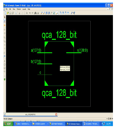 |
| The above diagram shows the representation of block diagram for 128 bit QCA adder. Here the inputs are A and B. And S is considered as output. C is a Wire. The input is in the range of (127:0). Since it is a 128 bit adder designed by using QCA. Hence the input given is 128 bit. |
RTL SCHEMATIC |
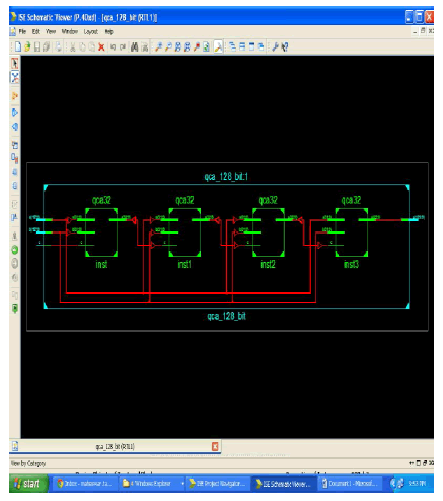 |
| The above diagram shows the RTL Schematic representation for 128 bit QCA adder. Here the four 32 bit QCA block are combined together to form a 128 bit QCA adder. The inputs are A and B. All the inputs (A and B) are connected serially. The ouptut of 1st block is connected to the C wire. This RTL Schematic block is obtained by using Xilinx. |
TECHNOLOGY SCHEMATIC FOR 64 BIT ADDER |
 |
| The above diagram shows the Technology Schematic for 64 bit adder. This can be obtained by using Xilinx. It consists of more number of adders. The operation of this can be explained in the above RTL Schmeatic. |
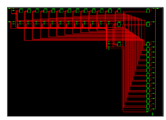
TECHNOLOGY SCHEMATIC FOR 128 BIT ADDER |
 |
| The above diagram shows the Technology Schematic for 128 bit adder. This can be obtained by using Xilinx. It consists of more number of adders when compared to 64 bit adder. |
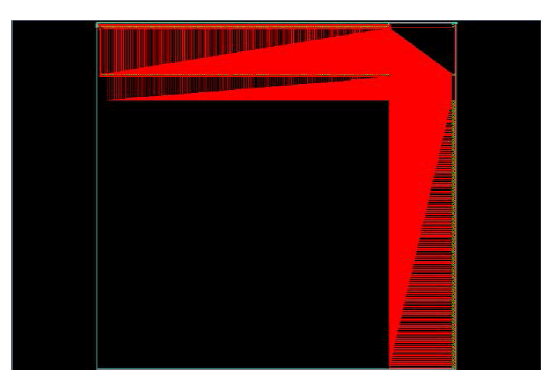
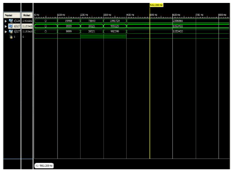
SIMULAITON OUTPUT OF 128 BIT ADDER |
| The simulation output for 128 bit adder is given below. The simulation results shows that the 128 bit QCA adder calculated how much delays are occured and it reduced the number of cell count when compared to other existing adders. |
 |
VIII. CONCLUSION |
| We have implemented a new 128 bit adder designed in QCA. It achieved performance of high speed when compared to all the existing QCA adders, with an area needed is cheap comparable with the RCA and CFA. Also the cell count required is less when compared to 64 bit adder. The unnecessary clock phases are avoided due the adopted basic logic and layout strategy. A 128 bit binary adder is designed in QCA and as described brief. Hence, the QCA architecture is therefore, low area, low delay, simple and efficient for VLSI hardware implementation. |
References |
|