International Journal of Innovative Research in Science, Engineering and Technology
ISSN ONLINE(2319-8753)PRINT(2347-6710)
ISSN ONLINE(2319-8753)PRINT(2347-6710)
M.Kavitha1*, C.Gopinathan2, R.Chandramohan3, K.Neyvasagam1** and P.Pandi4
|
| Related article at Pubmed, Scholar Google |
Visit for more related articles at International Journal of Innovative Research in Science, Engineering and Technology
Multilayer thin films have been prepared by chemical bath deposition technique. The films depend on the bath parameter like pH, temperature and time duration. Film has differentiate the three way and then coated on the ITO substrate .The composition of the thin film material like ITO/CdS/ZnS, ITO/CdS/ZnS/ZnO and ITO/CdS/ZnS/TiO2 /ZnO and ZnO is acted the buffer layer. The main objective of the work this material is acted on the photovoltaic solar cell material. A characteristics study on material is XRD, UV, PL, SEM and J-V characterisation. From the XRD, has analysed the structural parameters like grain size, micro strain value and dislocation density. The energy transition and optical parameter are carried out by UV studies. Photon emission and excitation in near the energy band can identified the PL studies and specified the quantum yield position is 0.999. The surface morphological has studied in the SEM data. J-V characteristics are studied and found the efficiency of the photovoltaic cell is increased. So the material acted the photovoltaic solar cell material by low cost technique. These results are reported
Keywords |
| ITO/CdS/ZnS/Al, ITO/CdS/ZnS/ZnO/Al and ITO/CdS/ZnS/TiO2 /ZnO/Al thin films, XRD, UV, PL, SEM and J-V Characteristics studies. |
INTRODUCTION |
| Recent trend the energy sources are demand overall the world due to the rapid decay of fossil fuels disturbing the economy of all counties in the world. Solar energy can be a major source of power then the potential is 178 billion MW, which is about 20,000 times the worldâÃâ¬ÃŸs demand is utilised but so far it remains too developed on a large scale. In general, the solar cell which consists of a substrate to hold on the thin film layer and TCO (ITO) to draw the current into the equivalent circuit. The buffer layer material is create the junction with absorber layer for generating carriers on absorbing light with minimal transmission or reflection losses and metal contact layer as the bottom electrode. In optical communication systems multilayer thin film coating materials is used in several applications and performing many functions such as antireflection coatings, frequency division multiplexing filters, interleaves, band splitting filters. Multilayer thin films show different physical properties other than the conventional monolayer thin films. In solar cell application is using the multilayer thin film material are obtained with attention due to the possibility of achieving reasonable conversion efficiency, stability and availability of low cost solar cells. |
II. EXPERIMENTAL |
| In the experimental design of the multilayer film has been prepared in the chemical bath deposition technique. An exterior bath is heated by a hot plate, was used to evenly distribution of temperature around a 1000ml deposition beaker. Samples were held vertically by Teflon clamps and stirring was maintained using magnetic stirrer during preparation. An ITO substrate is used for layer of deposition. Once the deposition take places the sample were cleaned with acetone solution. For the first layer of CdS deposition is taken 50 ml of 0.015M cadmium acetate, 25 ml of 1.5M thiourea were dissolved with 366ml of DI water. The solution mixture is poured in to a beaker which was heated and stirred until the temperature reaches 60oC and the pH is maintained from 8 to 9 by adding 213ml of 7.5M ammonia solution. The deposition was run over 1hr 30minutes and thus the CdS were deposited. The second layer of ZnS deposition is 50ml of 29.88g ZnSO4; 25ml of 22.84g thiourea were dissolved with 287ml of DI water. The solution mixture is poured in to a beaker which was heated and stirred and the pH is maintained from 11 to 12 by adding 213ml of 7.5M ammonia solution. The deposition was run over 1hr 30minutes and thus the ZnS were deposited. The third layer of ZnO deposition is 100ml of 2.2g zinc acetate, 25ml of 1.5M acetic acid added into the beaker which were heated and stirred until the temperature reaches 85oC. pH is maintained from 8 to 9 by adding of ammonium hydroxide solution and the deposition was run over the 2hr.The deposition of fourth layer TiO2 was prepared separately and added the third layer and then stirred until the temperature reaches 70oC.Upto four layer the solution was run over 6hr duration and its depends on the concentrate the bath parameters. |
III. RESULTS AND DISCUSSION STRUCTURAL STUDY |
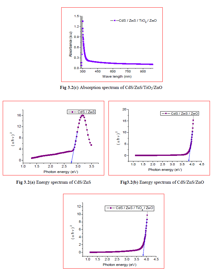
| The structural properties have been studies by X-ray diffraction technique using CuKα radiation source (λ=1.54056 Ao) with powder diffraction. The X-ray diffraction pattern of the film is chemically deposited onto ITO substrate as shown in figure 3.1. The maximum peak were observed and matched with the JCPDS data. The structural parameter were calculated from the XRD pattern and the film nature is orthorhombic and hexagonal structure and the grain size are determined by using Debye-SchererâÃâ¬ÃŸs formula is D = 0.9λ/β Cosθ. Where D is the gain sizes, β is the FWHM of the diffraction peak, θ is the Bragg diffracting angle and λ is the wavelength of x-ray. The dislocation density was calculated by the relation is δ = 1/ D2 and The micro strain was by the relation is ε = β Cosθ/4. These results are tabulated as seen in the table 3.1. |
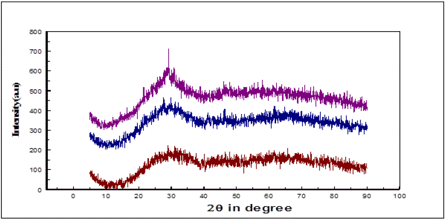 |
| Fig. 1Typical XRD pattern for ITO/CdS/ZnS/TiO2/ZnO/Al under deposited condition |
 |
UV STUDIES |
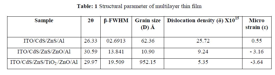
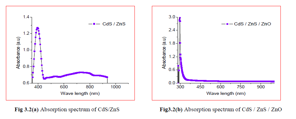
| The optical property of the multilayer film is study the physical phenomena and optical constant. The composition of film is having the different refractive indices and deposited on an ITO substrate. Such a system is applicable for the fabrication photovoltaic cell and optical devices. Multilayer film is possible for two o more wavelength of light to satisfy the conditions for low reflectivity of the film and the film system is considered the achromatised film. However for absorbing film is semi metallic films the refractive index n has to replace by n* (= n-jk). When a beam of a light passes through the medium it is partly transmitted, reflected and good absorption of the film. The absorption of the peak is narrow and estimated the band edge value. It is also calculated the optical thickness. These results are seen in the table 3.2 and Figure 3.2 as shown in the absorption spectrum and energy spectrum. |
 |
 |
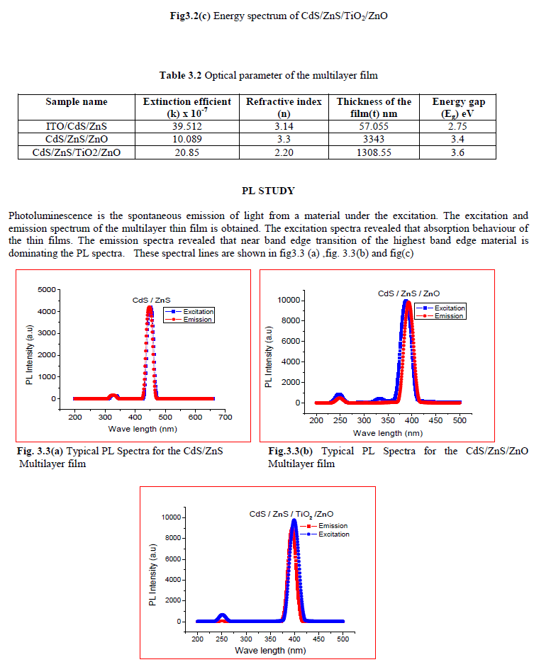 |
| Fig. 3.3(c) Typical PL Spectra for the CdS/ZnS/TiO2 /ZnO multilayer film |
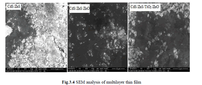
SEM ANALYSIS |
| The scanning electron microscope images have a good appearance and useful for judging the surface structure of the coated surface. The element in the film appears to be uniform with decreased porosity. The film exits as nano structure gain without any crack and pin hole on the surface. Morphology indicates that the substrate is almost complete covered spherical grain. The SEM picture as shown in the Fig.3.4 Fig. |
 |
J-V STUDY |
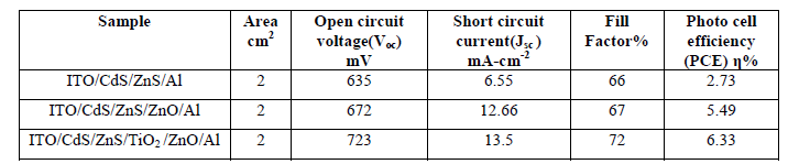
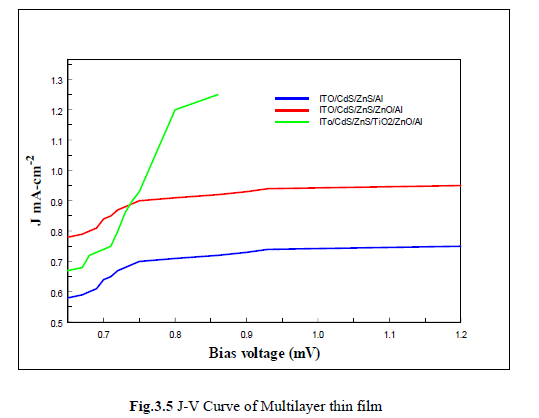
| A photovoltaic cell consists of a light absorbing material which is connected to an external circuit is an asymmetric manner. In the structure of ITO/CdS/ZnS/TiO2/ZnO/Al are designed and the J-V characteristics are measured and analyzed by the four parameter. This light driven the charge separation establishes a photo voltage at open circuit voltage is Voc, and generates a photocurrent at short circuit photo current is Jsc. J-V curve are shown in the Fig.3.5 and the efficiency are increased in the multilayer film and will use in the optoelectronic devices .These results are reported as seen in table 3.5. |
| Table 3.5 J-V parameter for multilayer |
 |
 |
IV. CONCLUSION |
| Multilayer thin films have been deposited onto ITO (TCO) substrate by CBD .The chemical bath deposition was used for the preparation of thin film of the important semiconductor. The effect of the deposition parameter on the structural, optical and electrical properties of the multilayer film was investigated. The structure of multilayer film was investigated by X-Ray diffraction pattern. The gain size, micro strain and dislocation density of the film was calculated from the XRD data. The optical absorbance and transmission studies reveal that the energy transition, Absorption band edge and thickness of the film. J-V graph plots of the multilayer films were carried out in illumination condition. The results are obtained multilayer thin films can be used as a photovoltaic material and the optoelectronics devices. |
References |
|