International Journal of Innovative Research in Science, Engineering and Technology
ISSN ONLINE(2319-8753)PRINT(2347-6710)
ISSN ONLINE(2319-8753)PRINT(2347-6710)
V. Cynthia Percy1 and R. Ramaprabha2
|
| Related article at Pubmed, Scholar Google |
Visit for more related articles at International Journal of Innovative Research in Science, Engineering and Technology
The field of telecommunication is booming up in a rapid manner and is always consorted with the growth of affirming equipments like power supplies. Efficient converters have to be used wherein the power quality is not deteriorated because of the interruption in the load. Here a three phase, single stage power factor correction converter is presented which has got distinguished features such as less distorted input current without deadband region and high power factor, less stress on switches and continuous output current for a wide range of load variation. Also this efficient converter is controlled using the conventional proportional-integral (PI) controller and fuzzy logic controller (FLC). The performance parameters are compared and found that FLC is more robust to parameter variations. The features, performance indices, simulation results obtained with the help of MatLab software are also presented.
Keywords |
| Telecom power supply, Three level converter, Single stage power factor correction, Control strategies, MatLab. |
INTRODUCTION |
| Telecommunications is one of the rapidly expanding fields in today’s world. This fast emersion in telecommunications field is always affiliated with development in supporting equipment like power supplies. Telecom power system is in the centre stage of how to provide authentic and cost effective power solution. The integral constituent of these infrastructures is the power electronics which is needed to provide the desirable design demands such as high reliability, efficient with less consumption of power and low cost [1]-[4]. The ac-dc converters have been used in almost all the fields but the conventional converters mounts way for highly distorted input current, resulting in a large amount of harmonics with a low power factor [5]. Due to the strict harmonic standards [6] such as IEC 61000-3-2, ANSI/IEEE-519 which was laid down, it was mandatory to prevent the rise of harmonics. In order to stick on to the harmonic regulations, a converter which is simpler in terms of topology with very less distortion, unity power factor and greater flexibility in the input current waveforms is also important. At higher power levels, three phase ac to dc switch mode rectifiers are normally used. The ac-dc converters needed to be more efficient with low cost due to its use in many off-line power supplies. For this, power factor correction (PFC) stages were added in front of the dc-dc converter. But this resulted in a two stage approach which allowed PFC stage to minimize the current distortion, followed by a dc-dc conversion stage, by which output voltage regulation can be performed. This seemed to be efficient but resulted complexity in control and efficiency was reduced. Then descended the single stage PFC circuits to annihilate the effects of the previous mentioned topology by which the PFC unit and dc-dc stage were made to share the same switch resulting in the elimination of controller and PFC switch. Electromagnetic interference (EMI) noise and stress across switches due to hard switching was a drawback again. Optimizing the design of the EMI filter was difficult in variable frequency control. Then a soft switching method was adapted to the dc-dc converter stage. Though zero voltage switching (ZVS) is achieved, increase in conduction loss led to the sacrifice of power factor. Lots of active and passive components were also needed [7]-[11]. These are the factors which contributed to the growth of high quality rectifiers. But in the existing rectifiers, input current distortion, high ripple current in output current, high stress on switches, sophisticated control techniques, complex design and high cost were some of the drawbacks. The growing number of loads that disturb the utility line, the resulting deterioration in power quality and the increasing consensus to consider power quality an important factor in the overall quality of life, lead to the recognition and development of an efficient converter with outstanding features. Owing to the above mentioned drawbacks in the previous topologies, a three phase, single stage power factor corrected multilevel type full bridge ac-dc converter [12] would be the best option for the telecom power supplies. |
CONVERTER DESCRIPTION |
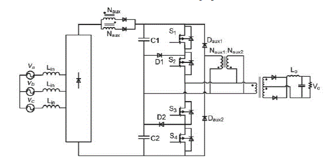
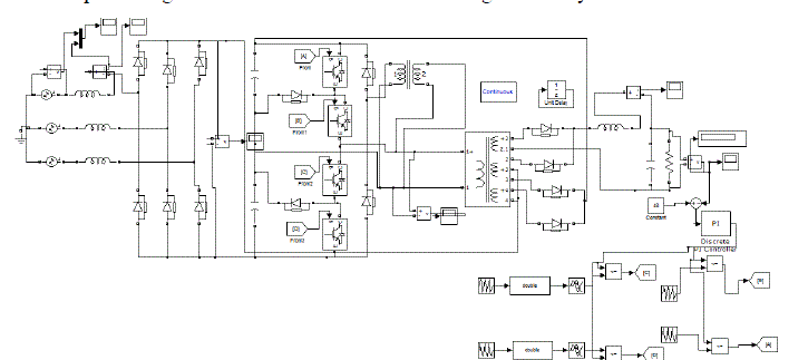
| The converter shown in Fig.1 consists of a three phase ac input section with an uncontrolled diode rectifier followed by the auxiliary windings taken from the converter main transformer. Then a multilevel type full bridge inverter is placed followed by the output transformer and the load. The basic principle behind the multilevel type full bridge converter is based on the combination of input inductors and auxiliary windings which carry out an action of PFC. The auxiliary windings which are the tertiary windings from the main converter transformer is used to cancel the voltage of the dc bus capacitors thereby working like a boost switch to produce a discontinuous input inductor current. This current can be further filtered to obtain a less distorted sinusoidal current with high power factor, devoid of deadband region [13]. |
 |
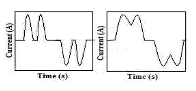
| Initially the rectifier which consists of six diodes is supplied by a balanced three phase voltage system. In each point two diodes of the diode bridge conduct resulting in an input current as shown in Fig.2 for discontinuous conduction mode (DCM) and continuous conduction mode (CCM) operation. The input current is zero in the time interval when the phase voltage is neither maximal nor minimal introducing deadband regions thereby making it non-sinusoidal and distorted. |
 |
| The next section in the converter is the auxiliary windings that are taken from the converter main transformer which performs PFC by acting like a boost switch with the input inductors. The alternate rise and fall of the input current in a switching cycle is similar to that of the inductor current in a boost converter [14]. Activating and deactivating the auxiliary winding is equivalent to the operation of turning on and turning off the boost converter switch in a boost converter correspondingly thereby making the current to be discontinuous. Thus PFC is achieved to improve the shape of input current. Next section is the multilevel type full bridge inverter (MLI) used for inversion [15]. Here the bus voltage is split among the capacitors equally; thereby reducing voltage stress. By this design the flexibility of the converter is improved. As a diode clamped multilevel converter (DCMLI) is chosen, technique of balancing the capacitor voltage is very important. Many techniques are provided in the literature [16]-[19]. Here a simple auxiliary circuit that is composed of a transformer with a turns ratio of Naux1/Naux2 = 1 and two diodes Daux1 and Daux2 has been used to assure equal voltage across the capacitors. Auxiliary circuit forces a diode to conduct thereby dissipating energy, when a difference in voltage is noted. By this means capacitor voltages are being balanced. |
DESIGN OF CONTROLLERS FOR THE CONVERTER |
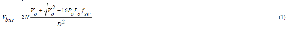
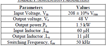
| The multilevel type full bridge converter is simulated in MatLab/Simulink Software. A three phase source with a line to line rms voltage of 208 ± 10% is connected with the input inductors. The value for Lin should be low to assure input current to be fully discontinuous but not very low value leading to high peak currents. The value calculated using the steady state analysis equations [20] and found to be 60 μH. Then the auxiliary windings are taken from the multi winding transformer block in MatLab. They are connected in an indirectly coupled fashion. The other end of the winding is connected to the full bridge converter of multilevel type. The full bridge converter consisting of four MOSFET switches which are connected like a diode clamped inverter. Next is the main transformer whose turns ratio, N should be calculated. Equations from (1) to (3) are used to calculate the turns ratio of transformer, where D is the duty ratio. The value of N is found to be 3. Hence the main transformer ratio is 3:1. The three level voltage is rectified using the transformer and then is filtered using an LC filter .The value of Lo is designed using (4) such that it results in a low ripple at output and low peak current rating for secondary diodes. The value of Lo chosen is 11 μH. The simulation parameters are tabulated in the Table I below. |
 |
 |
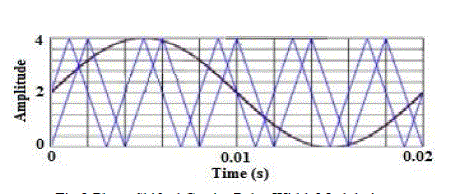
| The gating signals for the DCMLI are given through a phase shift PWM Technique (PSPWM) where the carrier waves are phase shifted [21] from each other by using (9). The technique of PSPWM is shown in Fig.3. Here a three level (m = 3) MLI is implemented and hence there are (m-1) two triangular carrier waves shifted by 1800 from each other. The gate signals are produced by comparing the modulating signal which is sinusoidal with the carrier signals. The phase shift is calculated by using (5). |
 |
 |
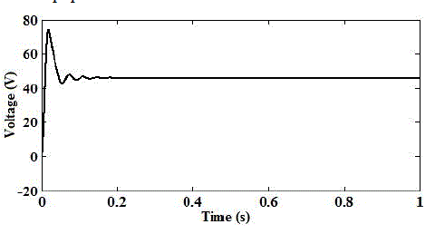
| Using the designed values, the converter is simulated and the parameters are analyzed [14]. The three level inverted voltage from the inverter is again rectified and filtered to obtain the constant DC output voltage of 48 V shown in Fig. 4 which can be powered to a telecom equipment. |
 |
| The converter experiences a high degree of non linearity in their control characteristics. They require a regulator to maintain the output voltage or output power constant in light of operational or environmental changes. For instance, the voltage of a power supply will tend to drop if load current increases. Similarly, changes in temperature affect the delivered power output. Therefore, there is an increasing need for a good controller to perform tight regulation under highly unpredictable load variation [22]. Here two control strategies namely the PI Controller and the FLC are studied and compared. |
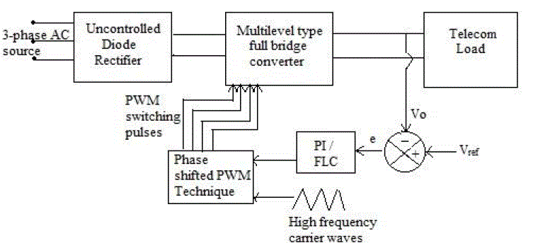 |
| The block diagram in Fig.5 shows the control strategy to regulate the output voltage. Under some variations, the error signal from the output voltage is compared using the reference voltage and it is processed using the controllers. The controlled signals are again compared with high frequency carrier waves and with the PSPWM technique, the PWM switching signals for the switches in multilevel type full bridge converter are generated. Thus the switching is controlled with respect to the variations. The controllers are tuned so that tight regulation is obtained. |
| A. PI Controller |
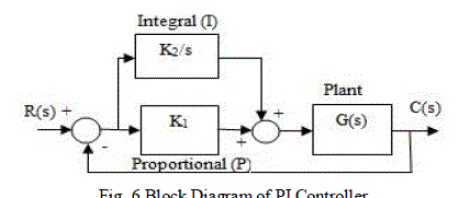
| PI control is a traditional linear control method used commonly in industrial applications. PI stands for the calculation that involves two separate parameters, the proportional and the integral. A PI controller is designed for operation during a steady state. Proportional term makes a change to the output that is proportional to the current error value. The contribution from integral term is proportional to both the magnitude of error and duration of error. By tuning the two constants in PI controller algorithm, the controller can provide control action designed for specific process requirement Fig.6 shows a block diagram of PI controller. In the proportional (P) control only gain adjustment is available to improve the system performance. The limitations on its ability to achieve both satisfactory accuracy and acceptable relative stability are understandable. If a P controller cannot meet the performance specifications, it should be replaced by a dynamic controller or a dynamic compensator to provide more flexibility. |
 |
| PI controller [23] is described by the transfer function in the continuous s-domain is given by (6) and (7). |
 |
| where Kp is the proportional gain; Ki is the integration co- efficient; Ti is integral action time or reset time. The values of Kp, Ki are evaluated using the automated tuning method. Fig.7 shows the implementation done using MatLab software. The output voltage becomes constant at a value of Kp = 0.05 and Ki = 68. It is found that the peak overshoot is eliminated and the output voltage remains constant after eliminating the steady state error. |
 |
| B. Fuzzy Logic Controller |
| The design of FLC [24] is primarily based on an expert knowledge, trial and error procedure. Number of linguistic variables, the base width of linguistic variables, the number of rules and slope of membership function (MF) affect the performance of controller. Unlike Boolean logic which the state value of any variable is either 0 or 1, fuzzy logic allows states between them. More specifically, that’s call membership value. The grade of membership value of fuzzy variable can be described in linguistic term. Fuzzy major features are the use of linguistic variables rather than numerical variables. Linguistic variables are defined as the variables whose values are define in a usual language (e.g. small and big), may be represented by fuzzy set. |
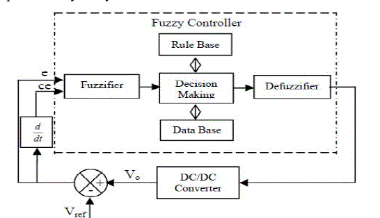 |
| The general structure of FLC controller is shows in Fig.8. That comprises four principal components: |
| 1) Fuzzifier: Fuzzification interface which converts input data into suitable linguistic values. |
| 2) Rule Base and Data Base: Both are known as knowledge base which consists of data base with necessary linguistic definition and control rule set. |
| 3) Decision Making: Decision making logic simulates a human decision process, infers the fuzzy control action from the knowledge of the control rules and the linguistic variable definition. |
| 4) Defuzzifier: Defuzzification interface yields a non fuzzy control action from an inferred fuzzy control action. |
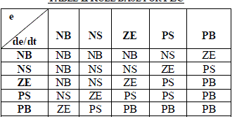
| The controller is designed based on the rules designed in the rule base. The rule base is given in Table II. |
 |
| Output voltage of both the controllers is analysed. Also the performance indices of the controllers are studied and the performance is compared. |
COMPARISON OF TWO CONTROLLERS BASED ON THE PERFORMANCE INDICES |
| The overall performance of the system is measured using certain specifications in respect of dynamic response to step input and steady state error. The desirable feature of these indexes is the selectivity i.e., its power to clearly distinguish between an optimum and non-optimum system and the ease of its analytical computation [25]. |
| A. Steady State Error: Steady-state error is the difference between the input and the output for a prescribed test input |
| →∞. |
| B. Integral Square Error (ISE): It has the ease that it is mathematically convenient both for analysis and computation. Minimization of ISE by adjusting system parameters is a good compromise between reduction of rise time to limit the effect of large initial error, reduction of peak overshoot and settling time. ISE is calculated by (8). |
 |
| C. Mean Squared Error (MSE): MSE measures the average of the squares of the errors. |
| D. Settling time: It is the time elapsed from the application of an ideal step input to the time at which output has entered and remained within a specified error band, usually about final value. |
| Fig.10 shows the output voltage obtained from PI and FLC. The settling time for a FLC is less compared to that of PI controller. The above mentioned performance indices were analyzed and tabulated in Table III. |
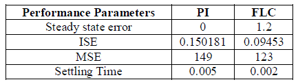 |
| From Fig.10 and Table II, It is inferred that FLC is more robust compared to that of PI. The indices ISE and MSE are also found to be low for an FLC. |
CONCLUSION |
| Telecom power system is in the centre stage of how to provide reliable and cost effective power solution. In order to adhere to the harmonic regulations a converter which is simpler in terms of topology with very less distortion and high power factor is presented in this paper along with the simulation results. It is simple in capacitor voltage balancing and can operate with less output inductor current ripple, even continuous output inductor current. It is operated with lower peak voltage stresses across the switches and the dc bus capacitors as it is a three level converter. This allows for greater flexibility in the design of the converter and ultimately improved performance. The converter is controlled using two strategies namely PI and FLC. It is found that FLC is more robust compared to PI controller based on the performance indices calculated. |
References |
|