International Journal of Innovative Research in Science, Engineering and Technology
ISSN ONLINE(2319-8753)PRINT(2347-6710)
ISSN ONLINE(2319-8753)PRINT(2347-6710)
Aparna.L.S, Jai Prakash Prasad
|
| Related article at Pubmed, Scholar Google |
Visit for more related articles at International Journal of Innovative Research in Science, Engineering and Technology
In this paper a technique to reduce the leakage power in the register file is presented. Power gating is one of the commonly used technique to reduce the subthreshold leakage current. But as the technology scales down, the effect of the leakage current increases since the supply voltage and the threshold voltage also has to be scaled down with technology scaling. With the power gating technique applied to the register file, it introduces a continuous leakage from the data retention element used to store the data. Since, it has to be powered up always to hold the data present in the register file. Thus an alternative technique called the supply switching with ground collapse technique (SSGC) is implemented where the supply is switched from the normally applied supply voltage to the lower voltage under the standby condition to reduce the leakage current compared to power gating technique. In this paper both of the above mentioned techniques is applied to the register file array of 8x8 with multiple read and write ports and leakage analysis is carried out in a Vdd=1V, 45nm CMOS technology. Also in this paper, the voltage and temperature variation is done to show the power variations.
Keywords |
| Leakage, Standby mode, Power gating, Register file, Low power. |
INTRODUCTION |
| Leakage current is one of the main concern. In high performance designs, the leakage power consumption becomes comparable to the switching power. Almost 40% of the power consumption is due to the leakage of transistors. This percentage increase with the technology scaling, thus leakage reduction technique has to be employed. In this paper the Supply switching with ground collapse technique is used to reduce the leakage current of the register file. Power gating is one of the commonly used technique where the power supply to the parts of the circuit which is not under use will be cut off. But in order to hold the data, the data retention flip flop has to be powered up always which results in the increase in the power dissipation under the standby mode. The subthreshold leakage increases considerably to great extent with this condition when the channel length is reduced. Thus, an alternative technique called supply switching with ground collapse technique is implemented on the register file. It overcomes the drawbacks of the data retention flip flop by switching to the lower supply voltage under the standby mode. Thus it reduces the leakage and this lower supply voltage will be sufficient enough to hold the data. |
| register file is an array of registers. It is implemented by using the fast static RAM’s with multiple ports. Since in the computers there will be multiple modules or devices which might want to read the data simultaneously and write the data, thus the multiple ports used enables the parallel computing capability. The SRAM used will have dedicated ports for read and write operation. Register file consists of the read and the write address lines and the corresponding data lines along with the Vdd and Vss. Register files usually has one word line per port, one bit line for read port and two bit lines for the write port. In this paper, a register file with 4 read ports and two write ports is used. In this paper, both the techniques are applied to the register file array of 8 register of 8 bits and the leakage analysis is carried out. |
LITERATURE SURVEY |
| By referring to [1], it proposes the use of transistor stacking effect and also it uses the multi threshold and the variable threshold CMOS techniques, where in the transistor stacking technique it uses the sleep transistors for reducing the leakage power in Cmos circuits. But the drawback with the use of Sleep transistor technique is that the area and the delay is increased and the state will be lost during the standby mode. Wong L.S.Y, Hossain S and Walker A [2] employs an active feedback loop to automatically cancel both junction and sub-threshold channel leakage. By reducing the effective leakage current, the capacitors used in the circuit can be significantly reduced, hence lowering the overall power consumption. Goto. M and Sato. T[3], propose a method of exploiting the characteristics of register renaming and the benefit from CMOS circuit techniques with sleep mode, can achieve leakage energy reduction. HeungJun Jeon, Yong-Bin Kim and Minsu Choi[4], uses the adaptive optimal reverse body-bias voltage technique that generates the optimal Vbody scaling during standby mode is used to reduce the overall leakage power. |
METHODOLOGY |
| The basic register file is implemented to which the power gating and the SSGC technique is applied. |
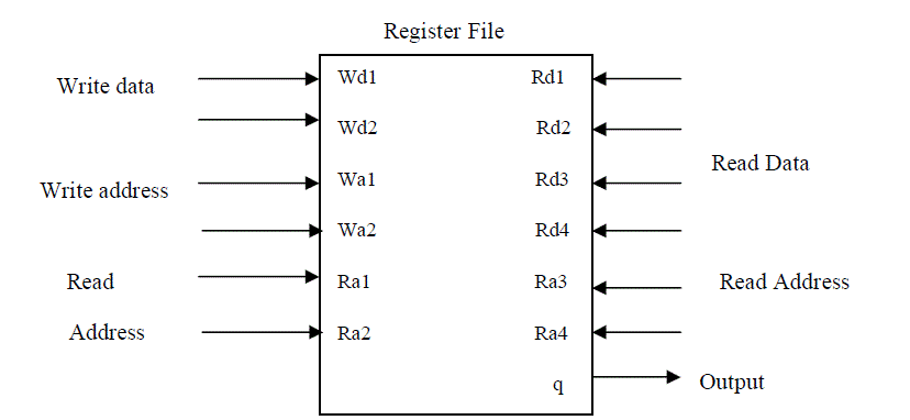
| 1. Basic Register File: The register file implemented here has mainly four read ports and two write ports respectively. It consists of the inverters connected back to back to store the data, the corresponding address lines and the data lines. It consists of 8 registers of 8 bits each. The representation is as shown in Fig 1. |
 |
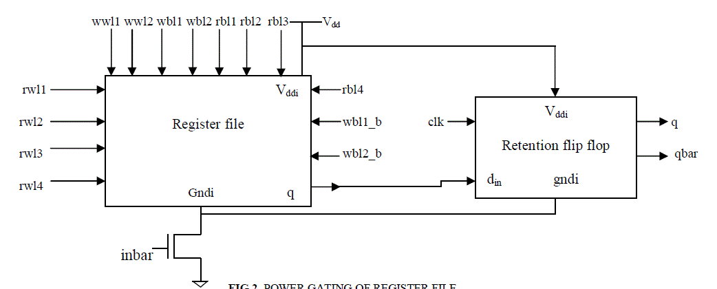
| 2. Power Gating Technique: The Power gating technique is used to shut down the part of the circuit which is not under use. It mainly uses a pmos header switch or nmos footer as sleep transistor to reduce the leakage current. This technique is applied to the Register file and is as shown in Fig. 2. |
 |
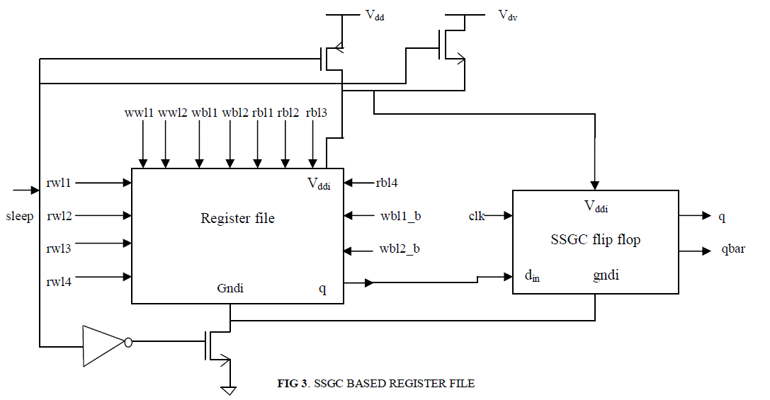
| 3. SSGC Technique: The Supply Switching with ground collapse technique (SSGC) is applied to the register file to reduce the leakage current under the standby mode. Here under the standby mode, the leakage current is reduced by switching over to the lower supply voltage Vdv as shown below in Figure 3. This technique mainly uses pmos header transistor, nmos header and other nmos footer transistors to operate under active and standby modes. |
 |
PROPOSED APPROACH |
| A. Operation of Register file. |
| The register file used here consists of four read and two write ports respectively. Fig .1 shows the implementation of the basic register file. Here, it is mainly used to perform the read and write operations. It is mainly used in programming the memory of computer system. The register file consists of the back to back connected inverters internally which is used to hold the data in the register file. Since, it consists of four read ports the corresponding address lines are named as rwl1, rwl2, rwl3 and rwl4 respectively. It consists of one bit line per read port which are rbl1, rbl2, rbl3 and rbl4 respectively. The read operation is performed by setting all the read bit lines high and the data present in the register file from the corresponding address line is read. The corresponding write addresses are wwl1 and wwl2 respectively. In case of the register file, there are two write bit lines corresponding to the write address lines. They are wbl1, wbl1_b, wbl2 and wbl2_b respectively. The write operation is performed by writing through the bit lines. For writing a 1, through write port 1 we set the bit lines corresponding to the write port 1 high, i.e setting wbl1 high and wbl1_b low. Then the word line, here wwl1 is asserted and the data to be written will be latched. |
| B. Design of SSGC flip flop and Data Retention Flip flop. |
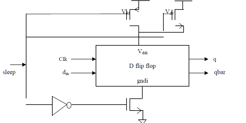
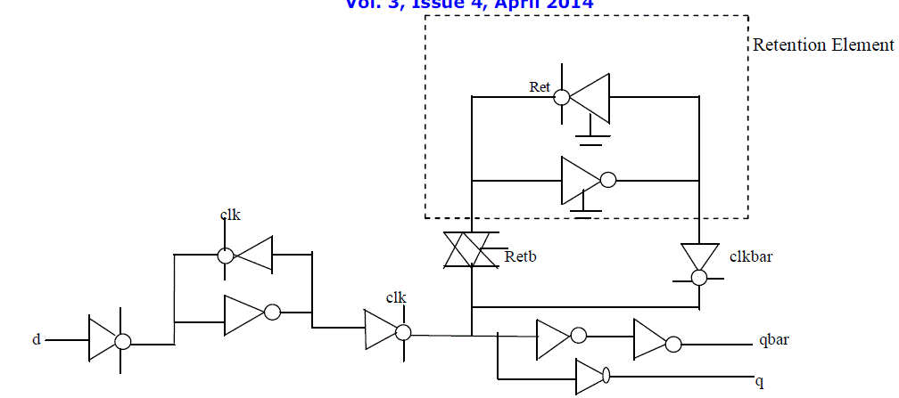
| (1) SSGC FLIP FLOP: The SSGC Flip flop is implemented using a D flip flop where the slave will be directly connected to Vss and all other components will be connected to the footer. The standby leakage will be reduced by restoring to lower voltage Vdv. The SSGC flip flop is implemented as shown in Fig. 4. Under the active mode, that is when sleep is 0, the Vdd = 1V is supplied through the pmos header and the nmos footer will be turned on, but at this stage the nmos header will be off. But under the standby mode, that is when sleep is 1, both the pmos header and the nmos footer will be off and the lower voltage Vdv is supplied through the nmos header to reduce the leakage current. The Vdv must be selected such that the voltage must be sufficient enough to hold the data. |
 |
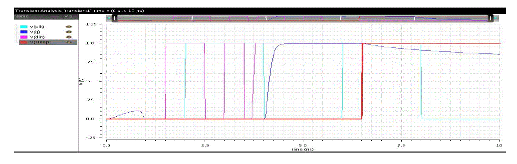
| The result of the design of the SSGC flip flop which holds the data is as shown in Fig 5. The data drops to a value of Vdvthreshold voltage. It shows that under the active mode, when sleep=0 it operates in the normal mode. The d flip flop is designed to be negative edge triggered, thus the output q follows the input din under the active mode. But under the standby mode, when sleep=1, we can observe that the output falls to some value which is Vdv-Vt value depending mainly upon the value of Vdv. |
 |
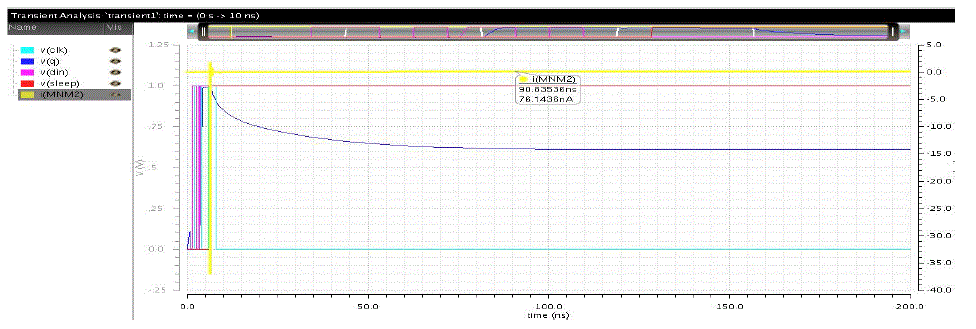
| To check whether the data is held (saturates to Vdv-Vt) or whether it loses the data, the transient time is increased to 200ns and is as shown in Fig 6 below. The leakage current is found to be 76.1436nA. |
 |
| (2) DATA RETENTION FLIP FLOP: The data retention flip flop is designed using the master and slave latches where the slave consists of the retention element which is nothing but back to back connected inverters which are directly connected to Vss. In order to hold the data, this flip flop always has to be powered up failing which it loses the data. But this is a big overhead since it induces continuous gate leakage which increases in the power dissipation under the standby mode. Thus this limitation is overcome by using the SSGC flip flop. The implementation is as shown in Fig 5. |
 |
| C. Operation of Power gated Register file |
| Power gating technique is applied to the 1 bit register file and the register file array of 8x8 which consists of 4 read and 2 write ports in this paper. There are two modes of operation which are active and the standby modes. Referring to Fig 2, under the active mode, Vdd is supplied to the circuit of the register file and data retention flip flop which performs the normal read and write operations. But under the standby mode, the data present in the register file has to be stored safely without losing it. The retention element present in the data retention flip flop holds the data. But the limitation is that since in order to hold the data, the data retention flip flop is always powered up(connected to Vdd) it results in the increase of the standby leakage current further causing the increase in the power dissipation. Furthermore, it also results in the increase in the wire length and the area. It worsens as the technology is scaled down. As the technology scales down bigger switches are needed since Vdd also has to be scaled down correspondingly with technology scaling. |
| D. Operation of SSGC based Register file |
| SSGC technique is applied to the 1 bit register file and the register file array of 8x8 which consists of 4 read and 2 write ports in this paper. It operates under two modes. Referring to fig 3, under the active mode that is when sleep is 0, the Vdd=1V is supplied through the pmos header switch and to the register file circuit and the SSGC flip flop and turns on the nmos footer switch. Under the active mode read and write operations takes place. But under the standby mode where no operation of read and write takes place, the data present in the register file must not be lost. Thus under this mode a lower supply voltage of Vdv is used which is minimum and sufficient enough to hold the data. The value of Vdv is taken to be 0.4 which is minimum value of the voltage sufficient to hold the data without losing it. This lower voltage suppresses both the gate leakage and the subthreshold leakage efficiently. |
SIMULATION AND RESULTS |
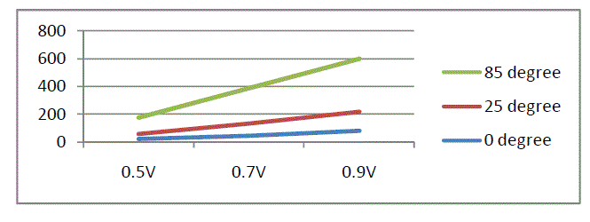
| Fig 8 shows the leakage current variation by varying Vdv. As the value of Vdv increases the leakage current also increases. Thus a minimum value of Vdv is set to reduce the leakage. It can be observed that lower is the value of Vdv the leakage saving will be more. But as the value of Vdv increases the leakage saving also decreases. Fig 9 and Fig 10 shows the simulation result for write and read operation on both the power gated and the SSGC implemented register file respectively which is carried out using the Cadence Virtuoso with Vdd of 1V. The propagation delay and current and for write operation for a 1-bit register file is found to be 14.541ps, 40.08μA respectively. Similarly the current and power consumption for read operation is found to be 17.847μA and 17.847μW respectively. On the other hand, the propagation delay and current and for write operation for a 8-bit register file is found to be 14.541ps, 287.13μA respectively. Similarly the current and power consumption for read operation is found to be 99.773μA and 99.773μW respectively. |
 |
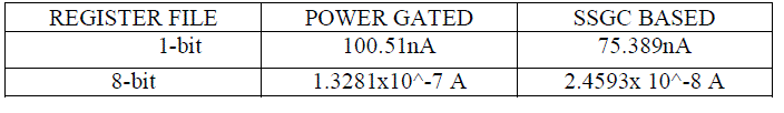
| The analysis of the leakage current is carried out in a register file of 1-bit and 8-bit with 4 read and 2 write ports respectively. It is as shown in the table 1 below. It can be seen that by comparing both the techniques, the supply switching with ground collapse technique provides less leakage under the standby mode compared to power gating technique. |
 |
CONCLUSION |
| As the technology scales down, leakage current increases significantly. Thus, in this paper it has been shown an alternative method to reduce the leakage which is the Supply switching with the ground collapse technique. This method is applied for implementation of low power register file of 1-bit and 8-bit with 4 read and 2 write ports in 45nm technology using the cadence virtuoso. It reduces the leakage current by a significant amount compared to power gating technique. Thus it can be used as an alternative in nanoscale CMOS technologies. |
References |
|