International Journal of Innovative Research in Science, Engineering and Technology
ISSN ONLINE(2319-8753)PRINT(2347-6710)
ISSN ONLINE(2319-8753)PRINT(2347-6710)
Abhinav Dogra1, Kanchan Pal2
|
| Related article at Pubmed, Scholar Google |
Visit for more related articles at International Journal of Innovative Research in Science, Engineering and Technology
Every Electronic circuit is assumed to operate off some supply voltage which is usually assumed to be constant. A voltage regulator is a power electronic circuit that maintains a constant output voltage irrespective of change in load current or line voltage. Many different types of voltage regulators with a variety of control schemes are used. With the increase in circuit complexity and improved technology a more severe requirement for accurate and fast regulation is desired. This has led to need for newer and more reliable design of dc-dc converters. The dc-dc converter inputs an unregulated dc voltage input and outputs a constant or regulated voltage. The regulators can be mainly classified into linear and switching regulators. All regulators have a power transfer stage and a control circuitry to sense the output voltage and adjust the power transfer stage to maintain the constant output voltage. Since a feedback loop is necessary to maintain regulation, some type of compensation is required to maintain loop stability. In this paper, a PI controller is designed and analyzed for a buck-boost converter. Stability analysis and selection of PI gains are based on the closed-loop error dynamics. PI controller, being the most widely used controller in industrial applications, needs efficient methods to control the different parameters of the plant. The output of the conventional PID system has a quite high overshoot and settling time.
Keywords |
| Buck-Boost converter, PI controller, PWM Duty cycle |
INTRODUCTION |
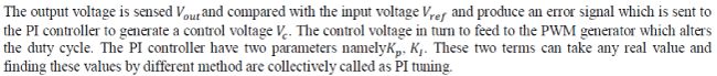
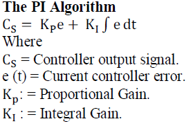
| A dc-dc converter is a vital part of alternative and renewable energy conversion, portable devices, and many industrial processes. It is essentially used to achieve a regulated DC voltage from an unregulated DC source which may be the output of a rectifier or a battery or a solar cell etc. Nevertheless, the variation in the source is significant, mainly because of the variation in the line voltage, running out of a battery etc., but within a specified limit. Taking all these into account, the objective is to regulate the voltage at a desired value while delivering to a widely varying load. A dc-dc switching regulator is known to be superior over a linear regulator mainly because of its better efficiency and higher current-driving capability. There are various topologies in the context of dc-dc converters the buck-boost converter are widely used. The basic circuit of buck-boost converter is shown in fig.1. The output voltage of a dc-dc converter is controlled by operating it in the closed loop, and altering its MOSFET (switch) gate signal accordingly. It is basically governed by a switching logic, thus constituting a set of subsystems depending upon the status (on-off) of the switch. In the well known pulse width modulation (PWM) technique, the control is accomplished by varying the duty ratio of an external fixed frequency clock through one or more feedback loops, whenever any parameter varies. PI controllers are the most widely-used type of controller for industrial applications. They are structurally simple and exhibit robust performance over a wide range of operating conditions. In the absence of the complete knowledge of the process these types of controllers are the most efficient of choices. |
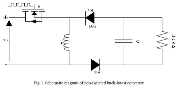 |
OPERATIONAL CIRCUIT FOR BUCK-BOOST CONVERTER |
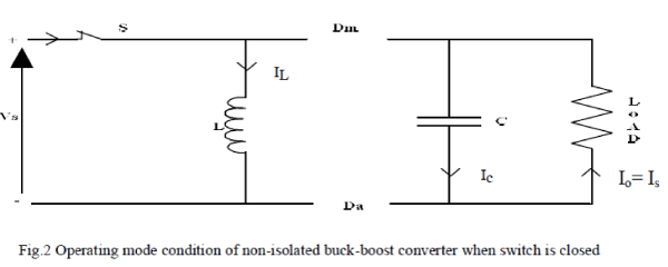
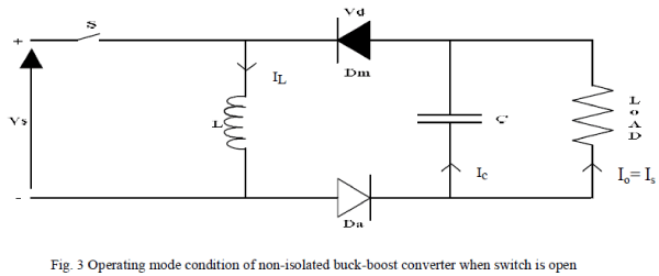
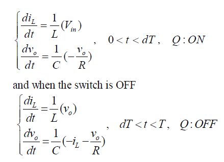
| The circuit operation divided into two modes. |
| Mode 1 (Switch is closed): When switch is closed then diodes Dïÿýïÿý and Dïÿýïÿý are reverse biased. The input current, which rises, flows through inductor L and switch S. This results accumulating energy in inductor L. The capacitor C discharges through load R. |
 |
| Mode 2 (Switch is open): When switch is open then the current, which was flowing through inductor L, would flow through L, C, Dïÿýïÿý, Dïÿýïÿý and the load. The energy stored in inductor L would be transferred to the capacitor and load, inductor current would fall until transistor switch Q is switched on again in the next cycle. |
 |
 |
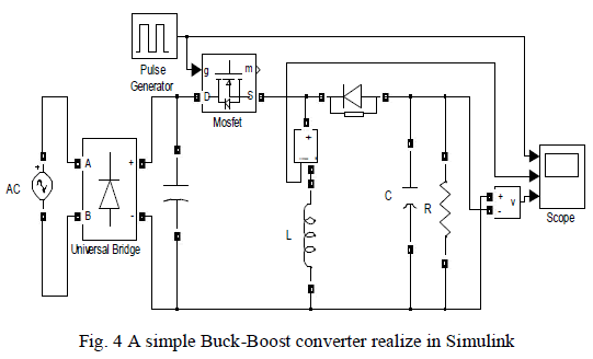
| In this Buck-Boost converter we have assume that the output voltage Vout = 400V. A simple Buck-Boost converter realize in MATLAB Simulink is shown in fig. 4. |
 |
| Design parameters and equations for non-isolated Buck-Boost Converter |
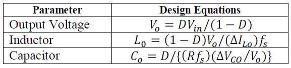 |
| Calculated value of design variables are L= 54.48 mH, C= 1.1248 μF and D= 0.5624. |
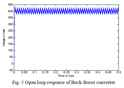 |
| The results of open loop Buck-Boost converter is shown in figure 5, which depict peak to peak ripple voltage (ΔVo) is 54 Volt and maximum overshoot of 10%. |
CLOSED LOOP BUCK-BOOST CONVERTER |
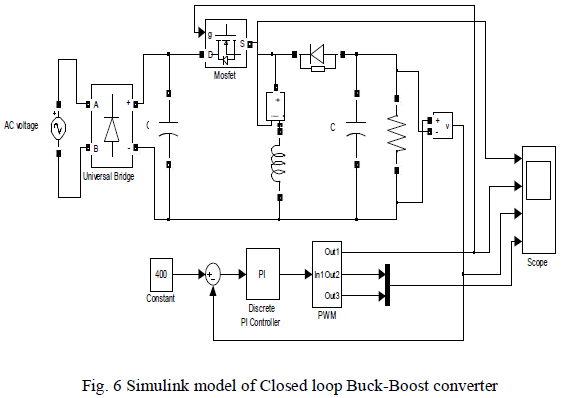
| The Simulink Schematic of Buck- Boost converter with analog PI controller is shown in fig. 6 |
 |
 |
 |
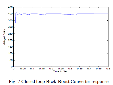 |
| The results of closed loop Buck-Boost converter is shown in figure 7 for KP= 0.0002 and KI= 0.029, which depict maximum overshoot of 3.25%, settling time 0.02ms and rise time 0.011ms. |
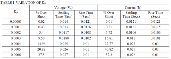
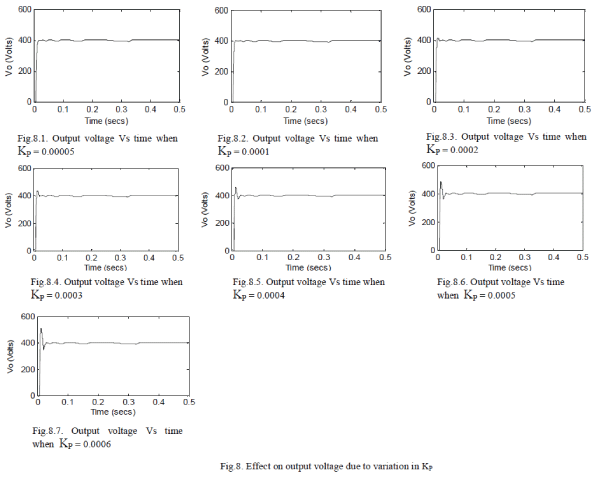
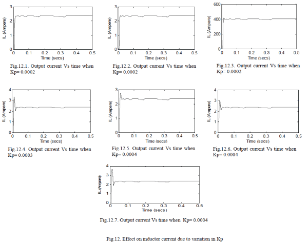
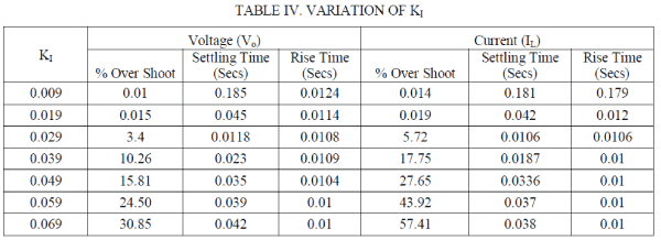
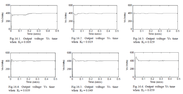
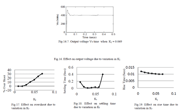
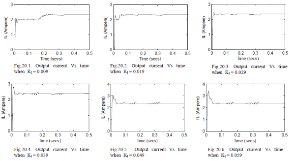
EFFECT DUE TO VARIATION OF KP AND KI ON OUTPUT VOLTAGE AND INDUCTOR CURRENT |
 |
 |
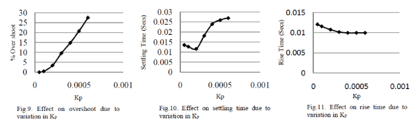 |
| When the value of Kïÿýïÿý increases up to three times of the designed values then output voltage overshoot and settling time continuously increases however rise time continuously decreases and finally attain a constant value. If value of Kïÿýïÿý decreases from its designed value then output voltage overshoot decreases however settling time and rise time increases. |
 |
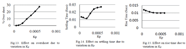 |
| When the value of Kïÿýïÿý increases three times of the designed values then inductor current (Iïÿýïÿý) overshoot and settling time continuously increases however rise time continuously decreases and finally attain a constant value. If value of Kïÿýïÿý decreases from its designed value then inductor current (Iïÿýïÿý) overshoot decreases however settling time and rise time increases. |
 |
 |
 |
| When the value of Kïÿýïÿý increases up to two times of the designed value then output voltage overshoot and settling time continuously increases however rise time continuously decreases and finally attain a constant value. If value of Kïÿýïÿý decreases from its designed value then output voltage overshoot decreases however settling time and rise time increases. |
 |
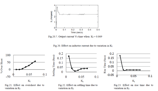 |
| When the value of Kïÿýïÿý increases up to two times of the designed value then inductor current (Iïÿýïÿý) overshoot and settling time continuously increases however rise time continuously decreases and finally attain a constant value. If value of Kïÿýïÿý decreases from its designed value then inductor current (Iïÿýïÿý) overshoot decreases however settling time and rise time increases. |
CONCLUSION |
| DC-DC converters and their design remain an interesting topic and new control schemes to achieve better regulation and fast transient response are continually developed. Step up switching regulators are the backbone of power electronic equipments. A key challenge to design switching regulators is to maintain almost constant output voltage within acceptable regulation. Performance and applicability of this converter is presented on the basis of simulation in MATLAB SIMULINK. The design concepts are validated through simulation and results obtained show that a closed loop system using buck-boost converter will be highly stable with high efficiency. Buck-Boost converter can be used for universal input voltage and wide output power range. The design of DC-DC converter capable of having low rise time, quick settling time and stable output. |
References |
|