Power consumption is considered as one of the important challenge in modern VLSI design along with area and speed consideration. Flip flop plays very important role in digital systems. In this paper comparative study of four different flip flops which includes pulse triggered as well as conditional technique flip flop such as IP-DCO, MHLFF, CPSFF, and CPFF topologies in sub threshold operation are examined. In recent years the ultra low power application can be possible using sub threshold technology. Using the advantage of this technology the power consumption of these flip flops is minimized. Sub threshold circuit consume less power than strong inversion circuit at the same frequency. Design is done using HSPICE in TSMC 180nm technology. The flip flops are analysed in all corners and parameters such as delay, power delay product, Energy delay product, and average power is measured at power supply voltage 300mV, and applied clock frequency is 1 MHz at temperature of 270C
Keywords |
| Sub threshold technology, flip flop, low power. |
INTRODUCTION |
| as stated by International Technology Roadmap for Semiconductor power consumption is considered as one of the
important challenge in VLSI along with speed and area consideration. Different ways for reducing the power consumption
have been proposed. In all these challenging methods minimizing power supply voltage gives direct and
effect on reducing power consumption [1]. Flip flops are major building blocks in digital VLSI system. The applications
areas where flip flops are majorly used are in registers, pipelines, state machines for sequencing data. Flip flop
have direct impact on power consumption and speed of VLSI system. Flip flop and latches consume more power because
of redundant transitions & clocking system which is included in it. Thus our aim is to design high performance
and also power efficient flip flop. One of the challenging methods to design low power flip flop is to use sub threshold
technology. |
| Power consumption of circuit depends on several factors such as data activity, frequency, supply
voltage, capacitance leakage and short circuit current. The total power dissipation is given by the sum of static and dynamic
power dissipation. Amongst them dynamic power is one of the important and it is given by, |
| PDynamic = 0.5. CL.VDD2.f ............................... (1) |
| Where α is the probability of signal transition within clock period, CL is the load capacitance, VDD is the power supply
voltage, f is clock frequency. Hence by reducing the power supply voltage there is tremendous reduction in power consumption
of circuit. |
| When supply voltage VDD reduces below the transistor threshold voltage VT, it is said to operate in
sub threshold region. This is one of the efficient methods for low power application in which the performance is of secondary
importance [2][3]. As power supply voltage is reduced below the transistors supply voltage VT, the sub threshold
current slowly charges and discharges nodes for circuits logic function. This weak driving current limits the performance
but low energy operation can be achieved with reduced dynamic &leakage power, resulting in improving
battery life. In sub threshold region due to absence of conducting inversion channels, transistors behave differently than
in strong inversion region. Thus resulting circuit characteristics change accordingly. Sub threshold technology can be
used in various applications such as wearable medical equipments such as hearing aids & pace makers, wrist watch computers, self powered devices & wireless sensor networks.[4][5]. One more application of sub threshold circuits is in
bursty mode application, which is ideal for a long period of time. In sub threshold circuit it satisfies the ultra power
requirement. The reason behind this is that it uses leakage current for its operating switching current. This small leakage
current however affects the performance at which the circuit is operated.
Section II gives details of flip flops; Section III gives the simulation, Section IV gives the results, Section V conclusion. |
II. PROPOSED FLIP FLOP DESIGNS |
| As power consumed by clock distribution network & storage element is high, pulse triggered flip flop has
been considered as popular alternative to conventional master slave flip flop. Circuit simplicity and high speed is the
advantage of pulse triggered flip flop which is more advantageous for low power consumption of clock tree system.
One of the other alternatives to reduce power in flip flop is to reduce number of clocking transistors. So both
types of flip flops are taken in this paper and their result is compared by parameters such as average power, Power delay
product, time delay, number of transistors in new technology i.e. sub threshold technology. |
| A. Implicit Pulsed Data Closed To Output: |
| A P-FF consists of pulse generator to generate strobe signal & latch circuit to store the data. Implicit pulse
generation is more advantageous for power consideration because it first controls discharging path and then needs to
physically generate a pulse train. Fig 1 shows IP-DCO. It contains an AND logic pulse generator and semi dynamic
structured latch design. In these circuit inverters I5 & I6 are used to hold the data & inverters I7 & I8 are used to hold the
internal node X. Two practical problems exist in this design of IP-DCO. First during rising edge of clock signal nmos
transistors N2 and N3 are turned on. If data remains high, node X will be discharged on every rising edge of clock.
This leads to large switching power. The other problem is that node X controls two larger MOS transistors (P2 & N5).
The large capacitive load to nodeX causes speed and power performance degradation [6]. |
 |
| B. Modified Hybrid Latch Flip Flop: |
| In Modified Hybrid Latch flip flop shown in Fig 2, node transistors occur only when input has different logic
value in two successive clocks. It uses feedback to remember instead of depending charge on capacitor a static latch
structure. A static latch can remember as long as gate power is supplied. In MHLFF redundant transitions are avoided.
The MHLFF eliminates the problem of discharging at node X. In second stage of MHLFF it has simple static latch
structure. By using feedback path, unnecessary discharging problem of internal node is reduced [6] |
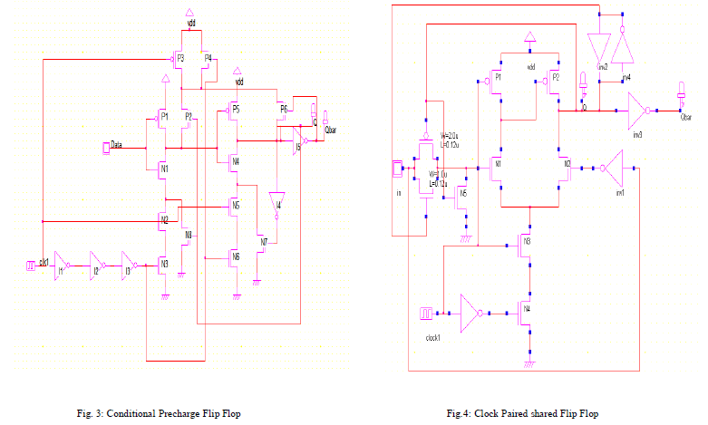
| C. Conditional Pre charge Flip Flop: |
| Conditional Precharge Flip Flop proposed [7] [8] and shown in Fig 3. In this odd numbers of inverters are
used in clock path to generate a transparency window as like in MHLFF. The important advantage of this work is
associated to preventing unconditional pre-charge operation of internal node, connected to excessive power dissipation
of circuit. This avoids the unnecessary transition of internal node as well as race condition at output. When D input is
high during transparency window it results in driving internal node to GND. It then sets the output Q to high level. As
internal node is at low level it remains at low level till input is at high level. To switch the internal node to high level
input transition should change from high to low in clock cycle. Internal node state is captured by second stage in flip
flop. When high to low transition occurs at internal node the low level is captured unconditionally and is synchronous
with clock edge. But the exception for this case is internal node transition which occurs after low to high switching
input when Q is at high level regardless of state of clock. Holding the output signal at desired level is done by use of
conditional keepers. When clock signal or delayed clock signal is low at that time high level output is held. Similar case
happens when output is at low level. |
 |
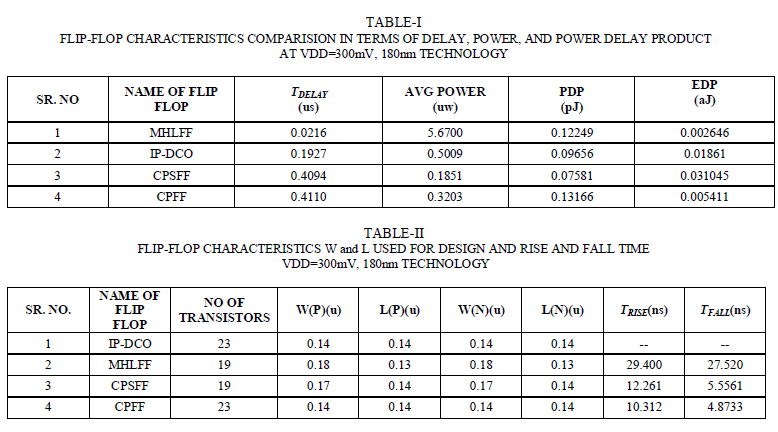
| D. Clock Paired Shared Flip Flop: |
| The Clock paired shared flip flop is proposed [9] uses less number of clocked transistors (i.e. only 4 out of
19 transistors) due to which clock load is decreased and it becomes efficient design. Hence it is improved version of
conditional data mapping flip flop. Clock pair transistors i.e. N3 and N4 are used for the first and second stage sharing
purpose. P1 transistor is used to charge internal node X which helps in avoiding floating problem. The flip flop operates
when CLK and CLKDB is at high logic..The working of CPSFF not only depends on data and clock but also on previous
input Q and Qb_kpr. So initial condition for working of CPSFF should be when D input is high, the previous state
of output should be low and the signal Qb_kpr should be high or all signals can be applied as vice versa. |
III. SIMULATION |
| A comparative study of above flip flop cells are performed with respect to parameters such as delay,
power consumption, power delay product, energy delay product. The simulation results for above types of flip flop
were obtained using HSPICE simulator. The operating conditions for design of the flip flop are VDD=300mV, clock
and input data frequency applied is 1MHz, temperature is 270C. The technology used for the flip flop design is TSMC
180 nm. The parasitic capacitances were extracted from layouts to simulate circuit accurately.
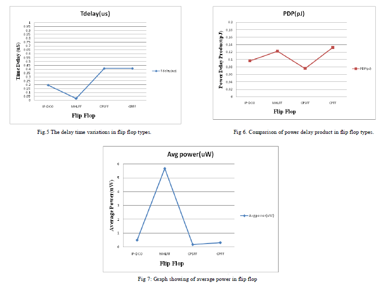
By eliminating parasitic capacitances we can avoid delay which depends on these capacitances and more over
power consumption also. Fig.5 shows the delay time variation of flip flops. It is seen fro the graph that MHLFF is
having less delay as compared to other flip flops. Fig. 5 shows the average power consumption of flip flop. The average
power consumption is very less in CPSFF and MHLFF is having higher power consumption in our all four flip flop
designs. Fig 6. Is having comparison of power delay product. Fig 7 gives the variations in average power for flip flop
types. The value of CPSFF is lower than other flip flops. It shows that CPSFF gives the best performance amongst
these four flip flops. Table- I and Table II shows the results of sub threshold flip flop in 180nm technology at
Vdd=0.3V |
 |
IV.RESULTS |
| Table –I shows the results of simulated flip flop. In these flip flops Modified Hybrid latch flip flop is having lower time delay
as compared to others. The average power of Clock Paired Shared flip flop is having lowest power consumption. Hence if power
consumption is considered the performance of CPSFF is better. The power delay product value is also best for CPSFF. Hence as
the comparison result is considered the CPSFF will give better performance than other three flip flops due to less number of
clocking transistors. The graphs for these results are shown below. It gives the detailed comparison of time delay , average
power and power delay product. |
 |
IV. CONCLUSION |
| In this paper flip flop designs i.e. Implicit Pulsed flip flop, Modified Hybrid Latch Flip Flop, Conditional Precharge and
Clock Paired Shared Flip Flop are discussed in sub threshold region in 180 nm technology. We can see from above discussion
that flip flop can still function well when power supply voltage reduces below its threshold voltage. In this firstly W/L ratio for transistors is not known. Hence different ratios would get different timing and power result. Secondly accuracy of technology
file can give different results. Here I have used 180nm technology PTM model. Hence different tool can give different result. To
get more improvement in results in future we can reduce the supply voltage and more over other technologies can be used. |
ACKNOWLEDGEMENT |
| I would like to thank Dr. A.K. Kureshi, for his unending support and wisdom urged me to pursue new ideas to implement in
my project. More over I would like to thank my teachers from VACOE, (E&TC) department for their support and guidance. |
References |
- J. Rabaey, M. Pedram, and P. Landman, Low Power Design Methodologies. Boston: Kluwer Academic Publishers, 1995.
- A. Wang and A. Chandrakasan, âÃâ¬ÃÅA 180 mV sub threshold FFT processor using a minimum energy design methodology,âÃâ¬Ã IEEE J. Solid-StateCircuits, vol. 40, pp. 310âÃâ¬Ãâ319, Jan. 2005
- R. M. Swanson and J. D. Meindl, âÃâ¬ÃÅIon-implanted complementary MOS transistors in low-voltage circuits,âÃâ¬Ã IEEE J. S. S. C., vol. 7, pp. 146âÃâ¬Ãâ153, Apr. 1972.
- H. Soeleman and K. Roy, âÃâ¬ÃÅUltra-low power digital sub threshold logic circuits,âÃâ¬Ã in Proc. Low Power Electronics and Design, 1999, pp. 94âÃâ¬Ãâ96.
- L. Nazhandali et al., âÃâ¬ÃÅEnergy optimization of sub threshold-voltage sensor network processors,âÃâ¬Ã in Proc. Intl. Symp. on Computer Architecture,2005, pp. 197âÃâ¬Ãâ207.
- Yin-Tsung Hwang, Jin-Fa Lin, and Ming-HwaSheu,âÃâ¬Ã Low-Power Pulse-Triggered Flip-Flop Design With Conditional Pulse-EnhancementSchemeâÃâ¬Ã IEEE Transactions On Very Large Scale Integration (VLSI) Systems, Vol. 20, No. 2, Feb
- N.Nedovic, M.Aleksic, V.G. Oklobdzijia, "Conditional Precharge Techniques for Power-Efficient Dual-Edge Clocking" Int. Symp. Low-PowerElectronics, Design, Monterey, CA, pp.56-59, Aug.2000
- Y. Zhang, H. Yang, and H. Wang, âÃâ¬ÃÅLow clock-swing conditional precharge flip-flop for more than 30% power reduction,âÃâ¬ÃÂElectron. Lett., vol.36, no. 9, pp. 785âÃâ¬Ãâ786, Apr.2000
- D. Markovic, B. Nikolic and R.W. Brodersen, "Analysis and design of low-energy flipflops," Int. Symp. Low Power Electronics and DESIGNPP 51-55 AUG 2001.
- N. H. E. Weste and D. Harris, CMOS VLSI Design - A Circuits and Systems Perspective Boston, MA: Addison Wesley, 2005.
- Predictive Technology Model
|