This work proposes a novel dual step-up converter fed with single stage capacitor commutated current source inverter with high voltage gain. In this context, power electronics performs important tasks making viable the connection of all these kind of clean power sources to the conventional grid and also to the load. This proposed system consists of two input sources, each one connected to two different inductor, being one fed by proton exchange membrane fuel cell and other fed by photovoltaic array. In this PEMFC act as storage system. The main feature of this capacitor commutated current source inverter is it can be switched between buck, boost, and buck-boost configuration. A modified carrier based modulation technique for the current source inverter is proposed to magnetize the dc-link inductor by shorting one of the bridge converter legs after every active switching cycle .This proposed system provide high voltage gain without use of a high frequency transformer which contribute to weight and size reduction in this proposed converter structure.
Keywords |
| Capacitor commutated current source
inverter, PEMFC, Photovoltaic array, Boost converter |
INTRODUCTION |
| Currently, alternative energy sources are seen as a matter of
great importance in many countries. This is because of
exhaustive carbon dioxide (CO2) emissions in the
atmosphere reaching alarming levels contributing, therefore
to global warming Sustainable development policies are
being put into practice, through which the use of alternative
and renewable energy sources have shown an increase in
their growth over non-renewable resources such as coal, oil
and alike. In this context of increasing renewable energy
sources, the development of power electronics plays its part,
more precisely in static power converters scene. |
| Due to the high growth rate of investments towards the
development and use of alternative sources of energy,
power electronics finds a broad market area, for example, in
the development of static converters used in power generation systems using photovoltaic panels to capture
solar energy and condition it into adequate energy [2].
It is worth noting that regardless of the type of
alternative energy source used (fuel cell, photovoltaic
panel, eolic energy, etc.), the use of static converters,
depending on the application, is essential to make it
possible to use these resources. Thus, the study of static
converters for application in systems based on
alternative energy is divided into two classes. |
| • Grid-Connected: systems where generated
power is injected into the distribution network |
| • Stand-Alone: systems where generated power
is supplied into a single load. This type of
application is attractive in places of difficult
access to energy distribution networks [2]. |
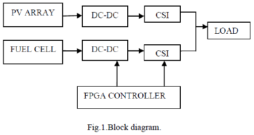 |
| Among the available renewable energy sources, the
photovoltaic (PV) system is considered to be a most
promising technology, because of its suitability in
distributed generation, satellite systems, and
transportation [3]. In distributed generation
applications, the PV system operates in two different
modes: grid-connected mode and island mode [4] -[8]. |
| In order to evaluate the effectiveness of the proposed
single stage high-voltage gain inverter structure fed by a
fuel cell, this is a well-known source of clean energy that provides energy through the use of electrochemical
processes [9], a proton exchange membrane fuel-cell
(PEMFC) was utilized. The PEMFC presents an inherent
characteristic which is the output voltage dependence of the
load current. This happens owing to internal losses, that is,
internal resistance ohmic losses, activation losses and
concentration losses [10]. |
| With this being the case, this paper, therefore sets as its
main objective contribution through the development of
static converters, which offers a reduction in size and weight
through a control strategy applied to a step-down/ step-up
DC–AC converter that operates with a totally controlled
input current and output voltage. The analyzed proposed
converter, portrayed in Fig. 2, consists of a single stage
structure fed by a fuel cell and is basically a boost converter
coupled to a current source inverter (CSI) targeted for standalone
systems. |
| The main differentiable feature observed in the proposed
structure is the ability to amplify voltage (24.48 VDC to
230VAC) without the presence of a pre-regulator stage or a
transformer. The high-voltage gain is possible through the
imposition of current in the input stage power source of the
inverter for a reference signal generated by a FPGA
controller. The use of a CSI structure arises from the
possibility of achieving instant variations of output voltage
as a function only of the energy stored in the input inductor.
Moreover, the CSI structure has some advantages, such as
the generation of sinusoidal voltage with low harmonic
distortion, which makes its connection to the network viable
[11, 14]. |
| Although the proposed single stage inverter operates with a
wide input voltage range (24–48 V), it is important to
consider a power decoupling technique such as an ultracapacitor
or a battery connected to the input to match the
oscillating output power to the constant input power
supplied by the fuel cell, as observed in this paper. Thus,
during transient load changes, the energy is provided by this
storage element suppressing, therefore the slow fuel cell
response and also avoiding the ‗starvation phenomenon‘
[17–19], which can lead to permanent damage of the
electro-catalyst of the fuel cell. |
| To achieve high voltage gain, this paper proposes a step-up
converter fed with single stage cc-csi ,the main feature of
this current source inverter is it has boosting ability it not
only convert dc –ac but also it step up voltage .It also called
as boost inverter . |
| This paper is organized as follows. The converter structures
are explained in section II. The PV array model and PEMFC
model is given in section III. Section IV describes Modified
carrier-based pulse width modulation. section V represents
the simulation results of the proposed system. |
CONVERTER STRUCTURE |
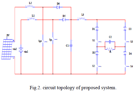
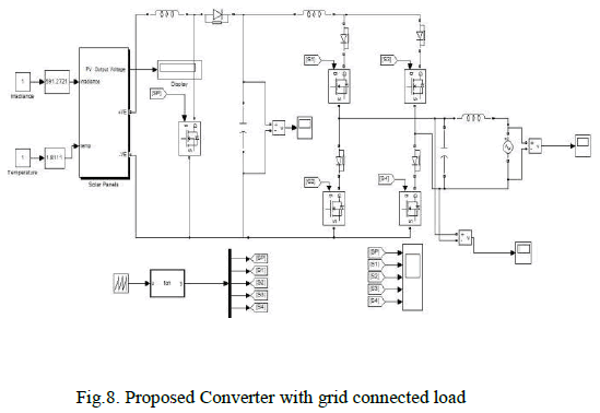
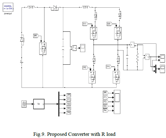
| The structure of the proposed dual step-up converter fed
with single stage cc-csi is represented in fig.2.As seen from
the figure, the converter fed with two input power sources.
Being one fed by PV array and other fed by PEMFC. The
main feature of the proposed system was the simultaneous
control of the input inductor current and output voltage and
its effectiveness has been proved in an inverter system feed by a PEMFC. Thus, one can conclude that the main
differentiable Feature observed in the proposed
structure was the ability to amplify voltage (24–70 VDC
to 230 VAC) without the presence of a dedicated pre
regulator stage or a transformer. On the other hand, the
main drawback of the proposed system is the high cost
of hydrogen, which is inherent in a PEMFC system. |
| In order to overcome this drawback and make the
proposed solution completely autonomous and reliable,
parallel connection of two dc sources is investigated in
this paper. In the converter structure, two inductors L1
and L2 make input power ports as two current type of
input power sources, which results in drawing smooth
dc currents from the input power sources, inductor L3 is
connected in series with single stage capacitor
commutated current source inverter to maintain a
constant current flow control. The inverter has four
metal oxide semiconductor field effect transistors
(MOSFET) (S1–S4) and four diodes (D1–D4). Each
diode is connected in series with an MOSFET switch
for reverse blocking capability. |
 |
| A. OPERATIN G PRINCIPLE |
| For one single dc source, as presented in [20],
the operating principle is based on the imposition of
two variables: |
| • IREF: Reference signal to the input current in
the Inductor |
| • VREF: Reference signal to the output voltage
of the Capacitor C. |
| For imposition of the variables IREF and VREF the
converter operates under the Current Control, described
in section II.A.1 cycle Control, described in section
II.A.2, and voltage control described in section II.A.3
respectively. |
| 1) Current Control |
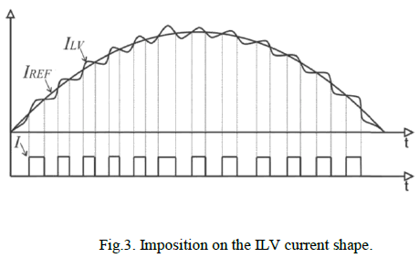
| This logic of control is responsible for enforcing
the desired current waveform across the inductor L and
is shown in Fig. 4 being represented by the I signal. The
ILV signal, sampled from inductor current, is compared
to the reference signal IREF, which is a voltage signal
generated from a microcontroller and converted to
analog form. The signal is a rectified sinusoidal voltage.
The result of the comparison between these two signals
is the I pulse. |
| • IREF > ILV: I IS A HIGH VOLTAGE LEVEL |
| • IREF < ILV: I is a low voltage level |
| 2) Cycle Control |
| This control is mainly intended to protect the switches
of the inverter circuit. A circuit fed by current source has a
characteristic such that an overvoltage occurs on the
terminals of an element that disrupts current flow. The
foreseen control always provides a way for the current of
the inverter circuit eliminating the possibility of overvoltage
across the terminals of the switches. |
| Another benefit occurs with the use of this control. The
switches S1 and S3 operate at low frequency, 60Hz,
reducing switching losses. |
 |
| The control logic consists of the comparison between
VREF and zero, generating two pulses that are
complementary as follows: |
| The comparison results generates two complementary
control pulses V+ that activates S1 and S4 and V- that
activates S3 and S2 working as follows: |
| • VREF > 0: Cycle+ is a high level of
voltage, Cycle- is a low level of voltage; |
| • VREF < 0: Cycle+ is a low voltage
level, Cycle- is a high voltage level |
| 3) Voltage Control |
| This is done by comparing VREF which is a
sinusoidal voltage signal, and VOV, sampled by a sensor.
The VREF signal is generated by the FPGA controller and
is synchronized with IREF. |
| Case: VREF < VOV: |
| • Cycle+ = 1, |
| • V- = 1; |
| Case: VREF>VOV: |
| • Cycle+ = 1, |
| • V + = 1; |
| B.MODE OF OPERATION |
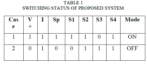
| The proposed system has only two operating
modes because of boost converter .The two modes of
operation of proposed system are |
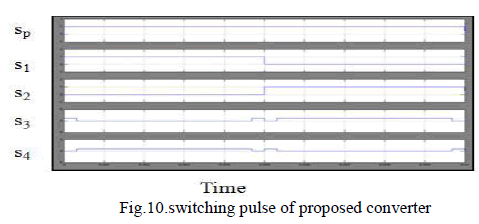
| • ON Mode |
| • OFF Mode |
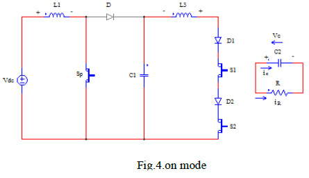
| a) ON Mode |
| When power device is on, L1 is connected to supply
Vdc and the inductor stores energy during on-time. The
diode D5 is reverse biased and isolates the output stage,
the inductor connected in series with current source
inverter will be discharging .The energy from the
inductor L3 will supply to the load. The switches Sp,
S1, S2 and S4 will be on, although switch S4 is active,
diode D4 is blocked by the capacitor and then the path
of least impedance to the circuit is provided by switch
S2. |
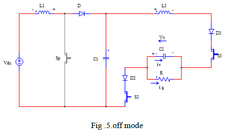
| b) OFF M ode |
| when power devices is off ,inductor L1 is discharging
and the diode D5 is forward biased and the inductor L3
is charging. During off time the load will get energy
from supply Vdc and inductor L1. The switch S2, S3, S4
will be on. |
 |
 |
 |
MODIFIED CARRIER-BASED PULSEWIDTH
MODULATION |
| Modified carrier-based pulse width modulation (CPWM)
is proposed to control the switching pattern for the single
stage CC- CSI. In order to provide a continuous path for the
dc-side current, at least one top switch in either arm and one
bottom switch must be turned ON during every switching
period. In conventional sinusoidal pulse width modulation
(SPWM), the existence of overlap time as the power devices
change states allows a continuous path for the dc current.
However, the overlap time is insufficient to energize the dclink
inductor, which results in increased THD. Therefore,
CPWM is proposed to provide sufficient short-circuit
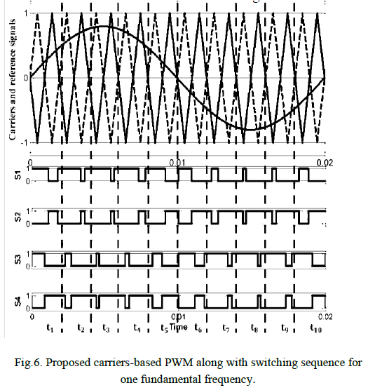
current after every active switching action. CPWM consists
of two carriers and one reference. Fig. 6 shows the reference
and carrier waveforms, along with the switching patterns.
The carrier with the solid straight line shown in Fig. 6 is
responsible for the upper switches, while the dashed line
carrier is responsible for the lower switches and is shifted by
180◦. To understand the switching patterns of the proposed
CPWM, Fig. 6 is divided into ten regions (t1 − t10), and
each region represents one carrier frequency period. CPWM
operates in two modes, a conductive mode and a null mode,
and the switching action of each MOSFET is equally
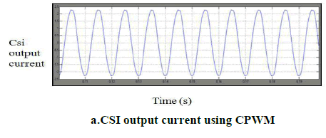
distributed during every fundamental period. To validate the
proposed CPWM, simulation results of a CSI operated by
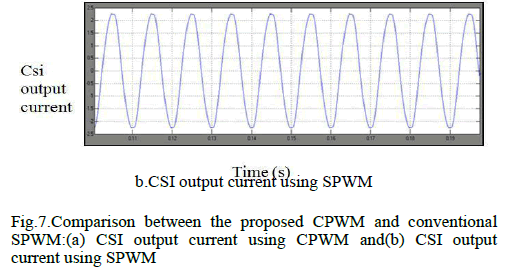
both CPWM and SPWM are shown in Fig.7. |
 |
 |
 |
SIMULATION DIAGRAM AND RESULTS |
 |
 |
Simulation specification |
| Output Voltage, VO RMS = 230v |
| Input Voltage - Fuel Cell System, VIN-1 = 22-50 |
| VDC Input Voltage - PV Array System, VIN-2 = 65 |
| VDC Input Inductor L1= 300μH, Core: 65-33-39 |
| Input Inductor L2= 300μH, Core: 65-33- |
| 39 Input Inductor L3= 300μH, Core: 65-
33-39 |
| Input capacitor C1=20 μF |
| Output Capacitor C = 20 μF |
| Switches, IRFP264 Diodes, STTH200L04TV |
 |
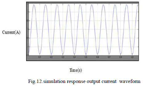
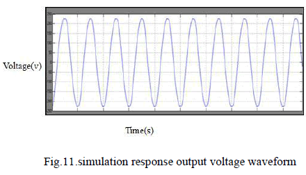 |
 |
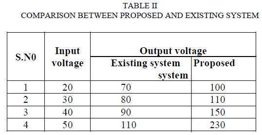 |
CONCLUSION |
| This project presented a novel single-stage inverter
topology called dual step-up converter fed with singlestage
capacitor commutated current source inverter and its
feasibility has been tested using two alternative energy
sources: a PEMFC and a PV array. High voltage gain and
totally controlled output voltage can be achieved by using
dedicated step-up dc–dc converter and not by using
transformer. Comparing to other autonomous inverter
structures, the proposed dual singles stage CC-CSI was
achieved adding only one extra diode, one switch, and also
one extra inductor. Despite the high cost of a PEMFC, like
most new technologies, its application in this kind of study is justified since it is a well- known source of clean
energy, contributing to the reduction of CO2
emissions. Therefore, the FC has been chosen as an
energy storage system in substitution to battery banks
commonly used in autonomous systems, eliminating
the obvious drawbacks related to lifetime and
maintenance issues. |
References |
- D.P.Kaundinya, P.Balachandra, N.H.Ravindranath.: “Gridconnectedversus stand-alone energy systems for decentralizedpowerâÃâ¬ÃâAreview of literatureâÃâ¬ÃÂ, Renewable and SustainableEnergy Reviews, 2009,13,(8),pp.2041-2050
- P.K. Steimer.: “Power electronics, a key techonology for futuremoreelectrical systems”, Proc. Of IEEE Energy ConversionCongress and Exposition, Atlanta, USA, September 2009, pp.1161 âÃâ¬Ãâ 1165.
- D.P.Kaundinya, P.Balachandra, N.H.Ravindranath.: “Gridconnectedversus stand-alone energy systems for decentralizedpowerâÃâ¬ÃâA review of literature”, Renewable and SustainableEnergy Reviews, 2009, 13,(8), pp. 2041 2050.
- M. G. Villalva, J. R. Gazoli, and E. R. Filho, “Comprehensiveapproach to modeling and simulation of photovoltaic arrays,”IEEE Trans. Power Electron., vol. 24, no. 5, pp. 1198âÃâ¬Ãâ1208,May 2009.
- K. Jong-Yul, J. Jin-Hong, K. Seul-Ki, C. Changhee, P. June Ho,K. Hak-Man, and N. Kee-Young, “Cooperative control strategyof energy storage system and microsources for stabilizing themicrogrid during islanded operation,” IEEE Trans. PowerElectron., vol. 25, no. 12, pp. 3037âÃâ¬Ãâ3048,Dec. 2010.
- Mehrizi-Sani and R. Iravani, “Potential-function based controlof a microgrid in islanded and grid-connected modes,”IEEETrans. Power Syst., vol. 25, no. 4, pp. 1883âÃâ¬Ãâ1891, Nov. 2010.
- W. Fei, J. L. Duarte, and M. A. M. Hendrix, “Grid-interfacingconverter systems with enhanced voltage quality for microgridapplication-concept and implementation,” IEEE Trans. PowerElectron., vol. 26, no. 12, pp. 3501âÃâ¬Ãâ3513, Dec. 2011.
- S. Dasgupta, S. K. Sahoo, S. K. Panda, and G. A. J.Amaratunga, “Single phase inverter-control techniques forinterfacing renewable energy sources with microgridâÃâ¬ÃâPart II:Series-connected inverter topology to mitigate voltage-relatedproblems along with active power flow control,” IEEE Trans.Power Electron., vol. 26, no. 3, pp. 732âÃâ¬Ãâ746, Mar. 2011.
- B. N. Alajmi, K. H. Ahmed, S. J. Finney, and B. W. Williams,“Fuzzylogic-control approach of a modified hill-climbingmethod for maximum power point in microgridstandalonephotovoltaic system,” IEEE Trans. Power Electron., vol. 26, no.4, pp. 1022âÃâ¬Ãâ1030, Apr. 2011.. 2041âÃâ¬Ãâ2050.
- Gopinath, R., Sangsun, K., Hahn, J.-H., Enjeti, P.N., Yeary,M.B.,Howze, J.W.: =Development of a low cost fuel cell invertersystem with DSP controlâÃâ¬ÃË, IEEE Trans. Power Electron., 2004,19, (5),pp. 1256âÃâ¬Ãâ1262.
- Avelar, H.J., Coelho, E.A.A., Camacho, J.R., Vieira Junior, J.B.,Freitas, L.C., Wu, M.: =PEM fuel cell dynamic model forelectronic circuit simulatorâÃâ¬ÃË. Electrical Power and Energy Conf.,October 2009, pp.1-6.
- Kang, F., Kim, C., Park, S., Park, H.: =Interface circuit forphotovoltaic system based on buck-boost current-source PWMinverterâÃâ¬ÃË. Proc. IEEE 28th Annual Conf. Ind. Electronic Society,November 2002, pp. 3257âÃâ¬Ãâ3261.
- M. Harfman-Todorovic, L. Palma, M. Chellappan, and P. Enjeti,“Design considerations for fuel cell powered UPS,” in Proc.IEEE Appl. Power Electron. Conf. Expo., 2008, pp. 1984âÃâ¬Ãâ1990
- E. Ribeiro, A. J. Marques Cardoso, and C. Boccaletti,“Fuelcellsupercapacitor system for telecommunications,” inProc. 5th IET Int.Conf. Power Electron., Mach. Drives, 2010,pp. 1âÃâ¬Ãâ6
- Gao, F., Liang, C., Loh, P.C., Blaabjerg, F.: =Diode-assistedbuck-boost current source invertersâÃâ¬ÃË. Int. Conf. PowerElectronic and Drive Systems, November 2007, pp. 1187âÃâ¬Ãâ1193
- M J V Vazquez, J M A Marquez, and F S Manzano, “AMethodology for Optimizing Stand-Alone PV-System IEEE TRANS. ON INDUSTRIAL ELECTRONICS, VOL. 55, NO. 7, JULY2008.
- S. K. Mazumder, M. Tahir, and K. Acharya, “MasterâÃâ¬Ãâslave currentsharing control of a parallel DCâÃâ¬ÃâDC converter system over an RFcommunication interface” , IEEE Trans. Ind. Electron., vol. 55, no.1,pp. 59âÃâ¬Ãâ66, Feb. 2008.
- Lacerda, V.S., Barbosa, P.G., Braga, H.A.C.: =A single-phasesinglestage,high power factor grid-connected PV system, withmaximum power point trackingâÃâ¬ÃË. IEEE Int. Conf. IndustrialTechnology, March 2010, pp. 871âÃâ¬Ãâ877
- Saha, A.K., Chowdhury, S.P., Chowdhury, S.: =PEM fuel cell asenergy source using fuzzy logic controllerâÃâ¬ÃË. IET-UK Int. Conf.,December 2007, pp. 288âÃâ¬Ãâ295.
- Kim, J., Jang, M., Cho, B., Tak, Y.: =Characteristic analysis andmodeling on PEMFC degradation associated with low frequencyripple current effectsâÃâ¬ÃË. IEEE Energy Conversion Congress andExposition, September 2011, pp.3336âÃâ¬Ãâ3342
- M. E. Schenck, J. Lai, and K. Stanton, “Fuel cell and powerconditioning system interactions,” in Proc. Appl. Power Electron.Conf. Expo., 2005, pp. 114âÃâ¬Ãâ120.
- M. Harfman-Todorovic, L. Palma, M. Chellappan, and P. Enjeti,“Design considerations for fuel cell powered UPS,” in Proc. IEEEAppl. Power Electron. Conf. Expo., 2008, pp.1984âÃâ¬Ãâ1990.
- E. Ribeiro, A. J. Marques Cardoso, and C. Boccaletti, “Fuelcellsupercapacitor system for telecommunications,” in Proc. 5th IETInt.Conf. Power Electron., Mach. Drives, 2010, pp. 1âÃâ¬Ãâ6.
|