ISSN ONLINE(2319-8753)PRINT(2347-6710)
ISSN ONLINE(2319-8753)PRINT(2347-6710)
Shailesh siddha1, Yashika Chander Pareek2
|
| Related article at Pubmed, Scholar Google |
Visit for more related articles at International Journal of Innovative Research in Science, Engineering and Technology
Integrated circuits are complex, containing both active and passive components that are manufactured on a single crystal chip of silicon and interconnected by wires. Chip sizes may vary from 2 mm to 800 mm. Integrated circuits contain insulating, semiconducting and conduction regions. These regions are combined in such a way to produce various electronic components like diode, transistor, MOSFET etc. Day by day I.C complexity has increased from small scale integration (SSI), to medium scale integration (MSI), to large scale integration (LSI), to very large scale integration (VLSI). The fabrication of I.C depends on material, process and design principals which form a highly developed semiconductor technology. Production of integrated circuit is a multistep sequential process like chemical cleaning, oxidation, etching, diffusion, photolithography etc. NMOS, CMOS, bipolar and integrated injection logic bipolar are major and complex I.C technologies. In this paper I explain the basic processing steps of forming number of PN Junction diodes on a single inch circular silicon wafer.
Keywords |
| IC- fabrication, Photo resist, RCA process, semiconductor,VLSI IC’s |
INTRODUCTION |
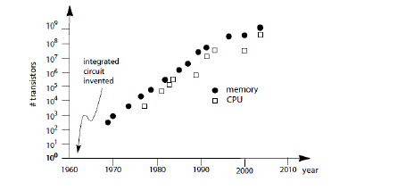
| The advent of integrated circuits made it possible to place a number of transistors and thus an entire circuit on a single chip. In the beginning these circuits had only few transistors but as the technology improved they became larger. Integrated circuits are manufactured on a silicon wafer. By 1970 it was possible to implement all circuitry needed to realize a microprocessor on a single chip [7]. In the 1960s Gordon Moore predicted that the number of transistors that could be manufactured on a chip would grow exponentially. His prediction now known as Moore’s Law [6] was remarkably prescient. Moore’s ultimate prediction was that transistor count would double every two years, an estimate that has held up remarkably well. Today, an industry group maintains the International Technology Roadmap for Semiconductors (ITRS) that map out strategies to maintain the pace of Moore’s Law. |
 |
WHY SILICON? |
| The basic semiconductor material used in device fabrication is Silicon. The success of the material is due to following reasons [4,5] |
| ïÃâ÷ Availability in large quantity in the form of SiO2 |
| ïÃâ÷ It has better physical characteristics and it can operate on a wide range of temperature (-700C to 1500C) |
| ïÃâ÷ Silicon has small leakage current in order of nanoampere that’s why silicon is more thermally stable (germanium has high leakage current in order of miliampere) |
| ïÃâ÷ High mobility ratio(2.6:1) so it has less switching time |
| ïÃâ÷ Mobility of majority charge carrier is high , it is suitable for high frequency |
| ïÃâ÷ It is possible to form a stable oxide (SiO2) silicon oxide has good insulating properties |
| ïÃâ÷ Silicon has no crystal defects (compound semiconductor GaAs has high density of crystal defects) |
| ïÃâ÷ Decomposition occurs in GaAs but not in silicon during processing steps |
| ïÃâ÷ Compound semiconductor is more difficult to grow in single crystal form |
STRUCTURE OF SILICON |
| Silicon as an element exists with three different microstructures: crystalline, polycrystalline, or amorphous. Polycrystalline, or simply “polysilicon,” and amorphous silicon are usually deposited as thin films with typical thicknesses below 5μm. Crystalline silicon substrates are commercially available as circular wafers with100-mm (4-in) and 150-mm (6-in) diameters [3, 5]. |
 |
| The primitive unit—the smallest repeating block—of the crystal lattice resembles a cube. The plane {111} has the highest density of atoms on the surface, so crystal grow is easy on this plane. Mechanical property like tensile strength is high in<111> direction processing characteristics like oxidation is also dependent on orientation. For example {111} is oxidized faster than {100} plane because they have more atom per unit surface. For bipolar circuits <111> orientation is preferred. MOS technology use silicon wafer with the crystal surface in hundred orientations because it introduce 10 times less interface trap density, which can charge Si-Sio2 interface. This charging introduces variation in threshold voltage which is undesirable [4]. |
FABRICATION FACILITIES |
| To successful manufacture a VLSI circuit, it is necessary to control cleanliness, temperature, humidity and orderliness. A. Pure water system |
| IC fabrication use large amount of water. Water contains impurities of sodium, copper and iron. These impurities can deposit on wafer during processing. There is a need of ultra pure deionized water. Water with specific resistivity 18MΩ-cm is considered to have a low ionic content. The resistivity of water is monitored by electrical means and particulate in water are monitored by automatic light block type of liquid borne particle centre [4]. |
| B. Clean room |
| All process steps are implemented in clean room. The air is maintained at a well controlled temperature and humidity level and is continuously filtered and recirculated. Air in the clean room is monitored and classified with respect to particulate. A “class 100” environment has a maximum of 100 particle per cubic foot with particle size larger than 0.5μm and a maximum of 10 particle per cubic foot with particle size larger than 5.0μm particulate can emanate from process equipment as well as from human; personal must wear proper clothing to protect the wafer[4]. |
FABRICATION PROCESS |
| Diode is a basic element in electronic and digital circuit. In this paper formation a PN junction diode is explained by VLSI fabrication steps which are stated below. |
| A. Silicon wafer cleaning (RCA process) |
| In the IC processing wafers it is necessary to maintain the purity and perfection of material. Silicon wafer is cleaned by standard RCA process. It useful to remove oil/grease, organic/ionic contamination, heavy metal ion and native oxide from the surface of wafer. Oil/grease/dust is removed by boiling wafer in trichloroethylene (TCE), acetone and methanol. Organic/ionic contamination is removed by boiling wafer in H2O:NH4OH:H2O2 (5:1:1) solution. Heavy metal ion is removed by boiling wafer in H2O: HCl: H2O2 (6:1:1) solution. Native oxide is removed by boiling wafer in HF: H2O (1:50) solution. Silicon wafer should rinse with deionized (DI) water after each acid step[2]. |
| B. Oxidation |
| Process by which a layer of silicon dioxide (SiO2) is grown on a silicon substrate is known as oxidation. This process is carried out in a furnace in high temperature. In this process dry wet dry oxidation is performed. When silicon wafers are heated in a pure oxidizing gas ambient such as dry oxygen it known is as Dry Oxidation. Oxide layers are very uniform but Dry oxide grows very slowly i.e oxidation rate is very low When silicon wafers are heated in an ambience of wet oxidizing gas such as oxygen bubbled through hot D.I Water (carrying steam vapors) it is known as wet oxidation. Growth rate is high but Quality of grown oxide is not very good. It is porous, i.e less dense compared to dry oxide [2]. |
| i) Advantages of Silicon Dioxide in IC Technology: There are several advantages of silicon dioxide in IC-technology such as |
| ïÃâ÷ Easily and selectively etched using photolithography techniques. |
| ïÃâ÷ Excellent masking behavior with most of the common impurity species, such as boron, phosphorus, arsenic and antimony. |
| ïÃâ÷ Excellent electrical insulator with resistivity values of the order of 1.0 X 10¹⁶ ïÃÂÃâ-cm and a band gap of 9.0 eV. |
| ïÃâ÷ Very high breakdown field, of the order of 1.0 X 10⁷ V/cm. |
| ïÃâ÷ Excellent junction passivation. |
| ïÃâ÷ Stable bulk electrical properties over a long period of time. |
| ïÃâ÷ Highly stable and reproducible interface states of Si-SiO2 interface with silicon[3,4] |
| C. Photolithography |
| In I.C Technology, photolithography is used to transfer patterns made on a mask to a semiconductor wafer. Therefore, to fabricate a device or an I.C, the oxide layer needed to be removed from the Selective regions on silicon wafer, where diffusion is desired. First silicon wafer is coated with photo resist and exposed in ultra violet light. By the application of photo resist oxide layer is etched [4]. Photo resist is an organic polymer, sensitive to UV light. It is temporarily coated on wafer surface to transfer design image on it through exposure in UV light.PR is applied to the oxidized wafer using a spinner. Spinner has vacuum holding arrangement and very high acceleration motor having adjustable speed (2000 to 6000 rpm). |
| (Positive photo resist is of Shipley-USA Microposit 1813 used in fabrication process) |
| (Negative photo resist is Kodak microeng 747 ) |
| D. Oxide etching |
| To remove SiO2 from regions exposed through photolithography is called oxide etching. After post bake, the wafer is dipped in Buffer HF solution for a particular time (determined by oxide thickness and etch rate) followed by thorough rinsing in D.I Water. It is called wet etching. To remove photo resist water cleaned wafer is boiled in acetone 2 min. to completely remove the photo resist from the wafer surface. If Wafer is subjected to Chemical Vapor Etching i.e subjected to a reacting gas mixture in a CVD reactor. It is called dry etching [4]. |
| E. Diffusion |
| As the given wafer is N type so we need to diffuse P type impurity into the wafer to create P-N junction and we take Boron (P type) impurity for diffusion. Boron activation, pre deposition of boron and oxidation is going on. During boron activation a layer of B2O3 is formed on BN wafer. After that silicon wafer is placed with BN wafer and boron will diffuse in to silicon wafer. During this process boro silicate glass is deposited so we need to etch the glass [3]. |
| Glass etchant 5ml BHF+85ml DI water+10ml HCl |
| BHF solution 40gm NH4F in 40ml of DI water+10ml HF |
| Material used for |
| Antimony diffusion Sb3Cl5 (antimony penta chloride) |
| Arsenic diffusion As2O3 (arsenic tri oxide) |
| Phosphorus diffusion POCl3 (phosphorus oxi chloride)[2] |
| F. Metallization |
| Metallization is the final step in the wafer processing sequence. Metallization is the process by which the components of IC’s are interconnected by aluminium conductor. This process produces a thin-film metal layer that will serve as the required conductor pattern for the interconnection of the various components on the chip. Another use of metallization is to produce metalized areas called bonding pads around the periphery of the chip to produce metalized areas for the bonding of wire leads from the package to the chip [4]. |
| Aluminium purity should be 5N (99.999%) |
| G. Photolithography |
| Photolithography is required for device isolation many devices can be fabricated in a single wafer. It is done by the same process as stated earlier photolithography process. |
| H. Metal Etching |
| Aluminum etching is done on the selective portion. It is done by the same process as stated earlier. |
| Aluminum etchant orthophosphoric acid |
| I. Annealing |
| First step in IC fabrication is to introduce dopant atom. Implantation damages the target and displaces atoms from its site. The electrical behavior after implantation is dominated by deep level electron and hole traps, which capture carriers and make the resistivity high. Annealing is the process which is used to repair the lattice damage by putting atoms on substitutional sites where they will be electrically active [4]. |
PROCESSING EFFECTS |
| After fabrication, wafer may be divided into regions with a very high portion of good chips and other regions where the yield of good chips is very low or zero. These effects include variations in the thickness of oxide, in the resistance of implanted layers, in the width of lithography, defined features, and in the registration of photo mask with respect to previous masking operations. Region where the polysilicon layer is thinner than average become over etched. Variation in the doping can lead to variation in the contact resistance in implanted layer. Variation in the thickness of deposit dielectric can lead variation in contact window sie. As advanced processes are developed which can eliminate or reduce these effects [4]? |
ADVANTAGE |
| ICs have three key advantages over digital circuits built from discrete components:- |
| A. Size |
| Integrated circuits are much smaller—both transistors and wires are shrunk to micrometer sizes, compared to the millimeter or centimeter scales of discrete components. Small size leads to advantages in speed and power consumption, since smaller components have smaller parasitic resistances, capacitances, and inductances. |
| B. Speed |
| Signals can be switched between logic 0 and logic 1 much quicker within a chip than they can between chips. Communication within a chip can occur hundreds of times faster than communication between chips. |
| C. Lower power consumption |
| Replacing a handful of standard parts with a single chip reduces total power consumption. Reducing power consumption has a ripple effect on the rest of the system: a smaller, cheaper power supply can be used; since less power consumption means less heat, a fan may no longer be necessary; a simpler cabinet with less shielding for electromagnetic shielding may be feasible, too[1]. |
CONCLUSION |
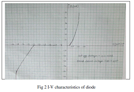
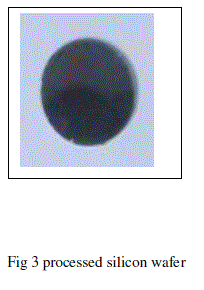
| I have explained entire fabrication process with practical implementation of PN-Junction Diode. I have fabricated approximately 12,500 diodes on a single inch circular silicon wafer by the use of earlier stated fabrication steps. Area of one diode is 200μm*200μm. cut off voltage is 0.3 volts and breakdown voltage is -18.7 volts. I-V characteristics of P-N junction diode are tested by IV probe method. |
 |
ACKNOWLEDGEMENT |
| It is my pleasure and privilege to acknowledge and express my deep sense of gratitude to my teacher and guide Prof R.P.Gupta(Ex-Director Grade scientist CEERI-Pilani)who inspired and initiated me to prepare this. He has always been kind enough to spare his valuable time and thought in giving necessary guidance. His rich and varied experience immensely helped me in understanding this topic clearly. |
References |
|