ISSN ONLINE(2319-8753)PRINT(2347-6710)
ISSN ONLINE(2319-8753)PRINT(2347-6710)
Lakshmi S.S1, Chandrasekhar N.S2
|
| Related article at Pubmed, Scholar Google |
Visit for more related articles at International Journal of Innovative Research in Science, Engineering and Technology
A soft-core processor is a model of hardware description language (HDL) of a specific processor (CPU) that can be customized for a given application and synthesized for an ASIC or FPGA target. Usually they contain embedded processors that are often in the form of soft-core processors that execute software code. This paper presents a FPGA implementation & verification of a pipelined MIPS 32-bit (microprocessor without interlocked pipeline stages) processor. In this technique soft- core does not requires any reloading or reimplementation of processor after the modification of MIPS code. The design consists of four major blocks: APB, UART, MIPS logic and software tool. The software tool sets the content of the instruction memory space of the processor without having to go through the FPGA implementation process. Soft-core processors are becoming popular solution to support application specific customization. the technique is being demonstrated by writing assembly code for an up/down counter using PERL script. The design architecture is coded using Verilog and realized in Spartan-6 FPGA using Xilinx ISE 14.2.based on the FPGA implementation results, the speed and performance of CPU can be increased
Keywords |
| FPGA, MIPS, APB, UART, PERL |
INTRODUCTION |
| A soft-core processor has many advantages compared to hard core processors in many applications like platform independence, reduced cost, low power consumption, flexibility and many more. . A major aspect of the MIPS design was to fit every sub-phase, including cache-access, of all instructions into one cycle, thereby removing any needs for interlocking, and permitting a single cycle throughput. The MIPS design was very much a typical RISC design. To save bits in the instruction word, RISC designs reduce the number of instructions to encode. |
| Due to its low complexity and easily extendable instruction set, it is easy to customize for special purposes and therefore it is ideal for implementation of specific applications. There are two approaches to implementing such a processor, the first approach being custom VLSI. This approach is a very expensive once-off approach. |
| The alternative approach is reconfigurable hardware by FPGA (Field Programmable Gate modified, which allows debugging and modification even once deployed. However, the run time loading for CPU on FPGA and its hardware realization using FPGA has not been reported in the literature. |
| The objective of this project is to propose a novel technique of run-time loading of machine code for MIPS-32 softcore processor on FPGA. In this technique, it sends the machine code to the instruction memory of the soft-core from the software tool through UART. The software tool is built using PERL (Program Extract and Report Language) script programming language. The user has to use the software tool to write MIPS assembly code, debug the code, generate the machine code and send it to the FPGA. |
RELATED WORK |
| In the paper “FPGA implementation and functional verification of pipelined MIPS processor” by authors Balaji Valli, Uday Kumar and Vijay Bhaskar, proposed the design of a pipelined MIPS processor using VHDL (Very High speed integrated circuit Hardware Description Language). In this implementation only the MIPS instruction format, instruction data path and decoder modules are analyzed. Instruction Fetch (IF) module is designed based on RISC CPU instructions, whose function is to fetch instructions by having synchronization with the control module and the arithmetic module, will check the validity of instruction module. Pipeline registers are placed into their respective VHDL module which generates the input to the particular pipelined register to implement the pipelined MIPS processor. |
| When the particular instruction moves to the instruction decode stage it will extract the saved value from the registers. The design used in this technique is top-down method and implemented by using VHDL. With reference to the paper “Soft core processors for embedded systems” by authors Jason G. Tong, Ian D.L. Anderson and Mohammed A.S. Khalid, described about the usage of soft core processors. Soft core processors can be customized for a given application as it has got more pros compared to hard core processors and also it can be synthesized on FPGA or ASIC. An embedded system contains embedded processors that are usually a soft core processor. The hardware platform of the embedded system consists of microprocessor, on-board memory, an output display and an input device to load the data and software. Many embedded system developers are facing time- to- market deadlines as it is very complicated to achieve smaller area with higher performance and lesser power consumption. Soft core processor holds many advantages like it is technology independent and can be synthesized to any target and therefore immune to become obsolete when compared with logic level description of a processor. |
| In the paper “MiniMIPS: An 8-bit MIPS in an FPGA for educational purpose” from the author Cezer Ortega- Sanchez from Curtin university, introduces an 8-bit implementation of MIPS single cycle architecture for education purpose. The user interface consists of only DIP switches, push buttons, LED’s and 7-segment displays. Program for the MiniMIPS must be written in assembly language, an editor and simulation tool was developed to support students in writing and verifying there programs. In MiniMIPS the original architecture was modified to make use of all the available peripherals. MiniMIPS has 8 registers and therefore 3 bits are sufficient to encode register operands and destination. |
| By considering the paper “Design and implementation of a 32-bit RISC processor on Xilinx FPGA” by authors Wael M Elmedany, Khalid A AlKooheji, has described about the technique called pipelining, which allows each instruction to be processed in specified number of stages. Pipelining technique allows parallel execution of instructions at various stages of pipelining. This type of processor finds its application in embedded controlled devices. This Harvard type of architecture can be used with two different memory spaces, a single dual port memory space and with separate data and instruction caches. RISC processors always use simple instructions and helps in fastest possible execution in one clock cycle. |
SYSTEM AND DESIGN |
| The system is divided into four major blocks: a software tool, an APB (Advanced Peripheral Bus) protocol, UART interface, and a microprocessor (MIPS 32-bit). This section each block will be discussed in detail. Fig. 1 illustrates the proposed system of the paper. |
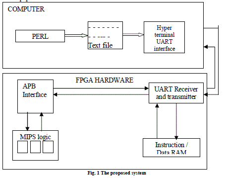 |
| Software tool: PERL is a family of high-level, general-purpose, interpreted, dynamic programming languages. The Perl languages borrow features from other programming languages including C, shell scripting. They provide powerful text processing facilities without the arbitrary data-length limits of many contemporary UNIX command line tools, facilitating easy manipulation of text files. Perl 5 is used for graphics programming, system programming and many other applications. In this paper PERL script language is used to generate Opcode for the MIPS processor. |
| APB protocol: The APB is part of the AMBA 3 protocol family. It provides a low-cost interface that is optimized for minimal power consumption and reduced interface complexity. The APB interfaces to any peripherals that are lowbandwidth and do not require the high performance of a pipelined bus interface. The APB has unpipelined protocol. All signal transitions are only related to the rising edge of the clock to enable the integration of APB peripherals easily into any design flow. Every transfer takes at least two cycles. |
| The protocol ensures that the following remain unchanged for the additional cycles: |
| 1. address, PADDR |
| 2. write signal, PWRITE |
| 3. Select signal, PSEL |
| 4. enable signal, PENABLE |
| Operating states of APB protocol: |
| The state machine operates through the following states: |
| IDLE This is the default state of the APB. |
| SETUP When a transfer is required the bus moves into the SETUP state, where the appropriate select signal, PSELx, is asserted. The bus only remains in the SETUP state for one clock cycle and always moves to the ACCESS state on the next rising edge of the clock. |
| ACCESS The enable signal, PENABLE, is asserted in the ACCESS state. |
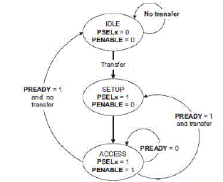 |
| If PREADY is held LOW by the slave then the peripheral bus remains in the ACCESS state. If PREADY is driven HIGH by the slave then the ACCESS state is exited and the bus returns to the IDLE state. |
| UART interface: A UART is usually an individual or integrated circuit used for serial communications over a computer or peripheral device serial port. UARTs are now commonly included in microcontrollers. The Universal Asynchronous Receiver/Transmitter (UART) takes bytes of data and transmits the individual bits in a sequential fashion. At the destination, a second UART re-assembles the bits into complete bytes. Each UART contains a shift register, which is the fundamental method of conversion between serial and parallel forms. Serial transmission of digital information (bits) through a single wire or other medium is less costly than parallel transmission through multiple wires. |
| The UART usually does not directly generate or receive the external signals used between different items of equipment. Separate interface devices are used to convert the logic level signals of the UART to and from the external signalling levels. External signals may be of many different forms. In this technique APB protocol is used for interfacing. |
MIPS ARCHITECTURE |
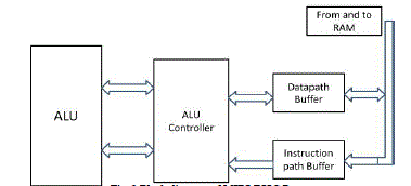
| The MIPS RISC processor presented in this paper consists of three components as shown in the fig.3.There mainly three components are: |
| Controller |
| Data path |
| RAM |
| Control unit allows each state to run at one clock cycle. The first state is the reset state followed by instruction fetching state and decoding state. The decoding state will also select the next state depending on the instruction, since every instruction has its own states. The control unit will jump to the correct state based on the instruction given. After all states of running instruction are finished, the last instruction will return to fetch state which will allow processing the next instruction in the program. |
| Data path model consists of the units necessary to perform all the operations on the data selected by the control unit. The model includes Register File, Arithmetic/Logic Unit, Memory Interface and Branching unit. |
| The ALU design consists of two input ports and one output port which mainly performs operations on two operands. It has a design similar to the control unit which selects an operation based on a code given by the ALUCL. |
 |
| The Memory interface is designing to accommodate simple load/store operations with the 16x32 memory. The effective address is calculated by adding the content of the address register and the immediate data. The Branch unit calculates a given condition by the control unit and raises a branch flag whether the condition is met or not, and if the flag is raised, it sends the branch address back to the control unit in order to replace the program counter. The Control lines coming from the control unit operate all the units in the Data path. |
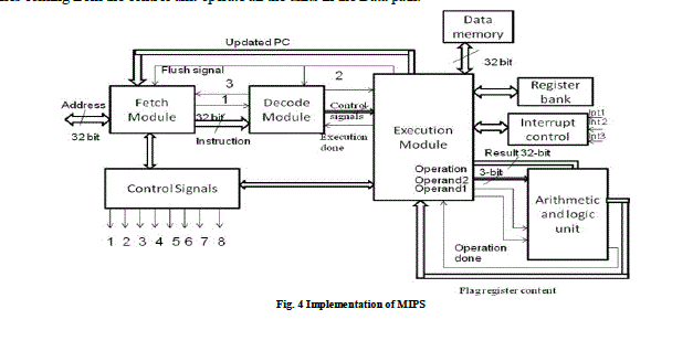 |
| MIPS (Microprocessor without Interlocked Pipeline Stages) intends to simplify processor design by eliminates hardware interlocks between 5 pipeline stages. Pipelining is the continuous overlapped movement of instruction to the processor. Result is an increase in the number of instruction that can be performed in a given time period. Processor is said to be fully pipelined if it can fetch the instruction on every cycle. |
| Stages of pipeline are: IF, ID, EX, MEM, WB. |
| Instruction Fetch (IF): To fetch the next instruction |
| Instruction Decode (ID): Decode the instruction and get the registers from the register file. |
| Execution (Ex): To perform the operation. |
| Memory Access (MEM): Perform the memory access and update the program counter. |
| Write Back (WB): write the results back to the files after completion of execution. |
| Single Cycle per instruction make logic and clock cycles usage simple. Uniform instruction format using a single word with the opcode in the same bit positions in every instruction demands less decoding. Simple addressing modes with complex addressing performed via sequences of arithmetic and/or load-store operations. Better performance compared to CISC. |
EXPERIMENTAL RESULTS |
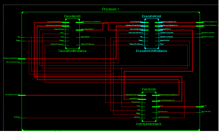
| By making use of software tools like ModelSim version 10.3, PERL scripting language and Xilinx version 14.3, it was possible to do analysis of the sub modules like RAM, APB, Fetch unit, Decode unit, Execution unit and also the top module i.e., MIPS processor module. |
| RAM module: Some of the internal signals of RAM are Address, Data_out, Read, Ready, Clock, Reset. Program memory made it rewritable in runtime, so bipartite the RAM (Random Access Memory) into nearly two equal sections. One section is for instruction memory and the other one is used as data memory approximately 2KB each. When WE (Write enable) =1, Write the data in to RAM. When WE (Write enable) =0, Read the data from the RAM. |
 |
| APB protocol: PSEL is high at the first pos edge of the clock. PENABLE should be high at the next pos edge of the clock. If it violates this condition it is called as protocol violation. Whenever the PREADY is high in the next cycle data will be available. |
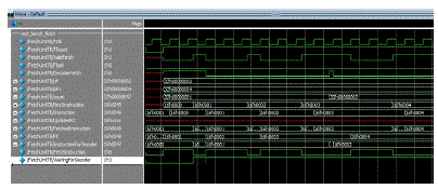 |
| Clk, Reset: Global signals. Valid fetch: It will fetch the valid instruction from the ram module through APB. Decoder fetch: Decoder sends this signal to fetch unit to send next fetched instruction. Flush: It will flush the entire module when jump or call instruction comes. Fetched Instruction: It will fetch the instruction (data and address) from the RAM. |
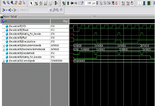 |
| Here transfer the instruction from instruction register to decode unit. In this unit the fetched instruction is decoded by the processor. It will get the operands and opcode given in the instruction. |
| Clk, Reset: Global signals. Waiting for decoder: when this signal is high, indicates that the fetch module is waiting for decoder to decode next instruction. Flush: It will flush the entire module when jump or call instruction. Instruction for decoder: Fetch unit sends 32-bit instruction to the decoder module. Execution done: After execution completes, execution module sends this signal to the decoder unit. |
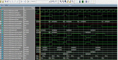
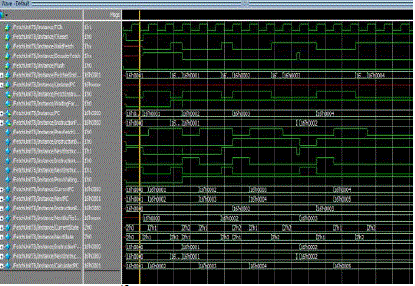
| Clk, Reset: Global signals. Waiting for execution: After completion of decoding it will wait for next execution. Control signals: It controls all instruction like opcode, fetch, program counter etc. Data memory request: Requesting for the data memory to store the data. Data memory operation: This stores required data in the data memory. Data memory address: This stores required address in the data memory. |
 |
 |
 |
CONCLUSION |
| In this paper, we have presented runtime loading of 32- bits MIPS soft core processor and UART. This processor is designed using HDL and it uses complete architecture of the MIPS processor and verified using simulation. The implementation results in less FPGA resource utilization and reduces area consumption when it is dumped on FPGA Spartan-3/Spartan-6 kit. Since it consumes less area in FPGA resource, we can utilize rest of FPGA resources to implement other parallel processors on the same device. The implementation is done using Up/Down counter assembly code as an example in GUI program to verify the microprocessor working and also focused on different optimization techniques such as pipelining in order to obtain high performance considering the parameters like speed, area and power. |
References |
|