International Journal of Innovative Research in Science, Engineering and Technology
ISSN ONLINE(2319-8753)PRINT(2347-6710)
ISSN ONLINE(2319-8753)PRINT(2347-6710)
V.Chanakya1,K.S.Murugesan2
|
| Related article at Pubmed, Scholar Google |
Visit for more related articles at International Journal of Innovative Research in Science, Engineering and Technology
The Combinational circuit designed was glitch free NAND-based digitally controlled delay-lines (DCDL) present a glitching problem which may limit their employ in many applications. The glitch free strobe-control based digitally controlled delay lines overcame this limitation by opening the employ of glitch free NAND-based DCDLs in a wide range of applications. The proposed glitch free strobe-control based digitally controlled delay lines maintains the same resolution and minimum delay of previously proposed glitch free NAND-based DCDL. Following this analysis, three driving circuits for the delay control-bits are also proposed. Proposed DCDLs have been designed in a 90-nm CMOS technology. Simulation results show that new circuits result in the lowest resolution, with a little worsening of the minimum delay with respect to the previously proposed DCDL with the lowest delay. Simulations also confirm the correctness of developed glitching model and sizing strategy. As example application, proposed DCDL is used to recognize an Alldigital spread-spectrum clock generator (SSCG). The use of proposed DCDL in this circuit allows to reduce the peak-to-peak absolute output jitter with respect to a SSCG using three-state inverter based DCDLs.
Index Terms |
| All-digital delay-locked loop (ADDLL), alldigital phase-locked loop (ADPLL), delay-line, digitally controlled oscillator (DCO), flip-flops, sense amplifier, spread-spectrum clock generator (SSCG). |
INTRODUCTION |
| In the recent deep-submicrometer CMOS processes, timedomain resolution of a digital signal is becoming higher than voltage resolution of analog signals [1]. This claim is nowadays pushing toward a new circuit design paradigm in which the traditional analog signal processing is expected to be progressively substituted by the processing of times in the digital domain. Within this novel pattern, digitally controlled delay lines (DCDL) should play the role of digital-toanalogconverters in traditional, analog-intensive, circuits. From a more practical point of view, nowadays, DCDLs are a key block in a number of applications, like all-digital PLL (ADPLL) [2]–[8], all-digital DLL (ADDLL) [9]–[11], alldigital spread-spectrum clock generators (SSCGs), [18]and ultra-wide band (UWB) receivers with ranging feature.Linear Feedback Shift Register is used to generate test vectors. It uses feedback and modifies itself on every rising edge of clock. A DCDL (Digitally Controlled Delay Lines) is using a delay-cells chain and a MUX to select the desired cell output. In these mux-based DCDLs, the MUX delay increases with the increase of the number of cells.The large time of MUXbased DCDLs can be reduced by using a tree-based multiplexer topology which results in an irregular structure which complicates layout design and consequently, also increases the nonlinearity of the DCDL.Different from the above approaches, in this DCDL topology each cell is constructed by using NAND gates. This apparently solves the trade-off related to the MUX of previous structures. A deepen analysis reveals that the input capacitance of the DCDL increases linearly with the number of cells. This clearly reintroduces a trade-off between the number of cells. In [2]–[5], the DCDL is constructed by using a regular cascade of equal delay elements (DE). In this circuit, the multiplexer of previous DCDL is theoretically spread among all cells. In this way the minimum delay is very low and becomes independent of the number of cells. In addition the highly regular topology allows a simple layout organization [8] which provides very low nonlinearity layout effects. Each DE in [2]–[5] is constructed by using only NAND gates, obtaining a very good linearity and resolution. The DCDL proposed in [8] uses again a structure of cascaded delay elements. Differently from [8]–[11], each element is constructed by using three-state inverters (TINV). Since the pull-up network of a TINV requires two series devices whereas a NAND gate uses a single device in the pull-up, we can expect that the resolution of this solution is higher than the resolution of NAND-based DCDLs. |
| The DCDL proposed in [1] is also based on a cascade of equal delay elements, which allows a simple layout organization. In this case each delay element is constructed by using an inverter and an inverting multiplexer. The inverter and mux topology have two drawbacks. A first weakness is due to the different delays of the inverter and the multiplexer which results in a mismatch between odd and even controlcodes. A second drawback is due to the large multiplexer delay, which provides a resolution higher than the resolution of both NAND based DCDLs and TINV-based DCDLs. Glitching is a common design problem in systems employing DCDLs. In the most common applications, DCDLs are employed to process clock signals, therefore a glitch-free operation is required. A necessary condition to avoid glitching is designing a DCDL which have no-glitch in presence of a delay control-code switching. This is an issue at the DCDLdesign level. Many approaches are known to avoid glitching in mux-based DCDLs. It is interesting to observe that the DCDL topologies of [8], from a logical point of view, correspond to distributed MUX-based structure. Glitching in these topologies can be avoided by using a thermometer code for the control-bits, or using the approach of [3]. On the other hand the NAND-based DCDL topology of [2]–[5] presents a glitching problem that, to the best of our knowledge, is still not known in Literature. It is worth to note that in the ADDLL topologies of the DCDL glitching is filtered by the phase detector and harmonic locking circuitry during locking phase. In other applications, however, the presence of this glitching phenomenon can substantially limit the employ of NANDbased DCDLs. This represents a substantial drawback of this topology in comparison to the solutions of [8] and [11].The errors that in some applications can originate from DCDL glitching will be also discussed within this paper.This paper gives two contributions to the design of NAND-based DCDLs. First it is shown and analyzed the glitching problem of the NAND-based DCDL .The proposed NAND-based DCDL allows to achieve a resolution, similarly to the NAND-based DCDL. The paper is organized as follows. In the same DCDLs in comparison to previously proposed structures. Finally, Section VI describes the employ of proposed DCDL to implement an All-digital SSCG designed with section the glitching problem of this DCDL is analyzed. The structure of proposed, glitch-free, NAND-based DCDL is presented in Section III. Section IV analyzes theoretically the novel DCDL structure by deriving the conditions (timing constraints) needed to avoid glitching in proposed circuit. These results are used to propose three different driving circuits for the delay control-bits of proposed DCDL. |
 |
PREVIOUSLY PROPOSED NAND-BASED DCDL AND GLITCHING |
| Fig. 1(b) shows that the structure exhibits a more severe glitching problem when the delay control-code is increased by more than 1.The analysis of the figure, in this case, reveals that, in the worst case, four paths propagate within the DCDL structure and may create a multiple-glitch at the delay-line output. When the control-code is increased, the logic state of the output becomes dependant on a portion of the DCDL for which and switch from 1 to a logic state dependant on In. This switching may determine output glitches. This consideration also demonstrates that no glitching can occur when the control-code is decreased. When the control-code is increased by one, the glitching problem could be avoided by delaying signals with respect to signals (see in Fig. 1(a). This solution, however, does not solve the glitching problem when the control-code is increased by more than one [see Fig. 1(b)].The Fig. 2 shows a transistor-level simulation of a NAND based DCDL composed by 64 elements. The control-code of the DCDL is firstly changed from 9 to 62 and, afterwards, changed back from 62 to 9. The DCDL output is reported in the third curve of the figure (“Out (NAND based [2]–[5])”). When the code word is increased ,it can be observed the presence of three glitches on the DCDL output. As observed before, when the code word is decreased, no output glitching occurs. The glitching problem in still more severe when the DCDL is closed in a ring-oscillator topology to build a DCO. Fig. shows the simulation of a ring-oscillator based DCO designed by using the NAND-based DCDL. It can be observed that the delay control-code is initially equal to 20, this corresponds to an oscillation frequency of about 500 MHz. When delay control-code is switched from 20 to 30 a glitch is produced by the DCDL. Because of the feedback topology of the DCO, this glitch remains entrapped in the ring-oscillator, providing a strong modification also of the steady-state response of the circuit. Substantially the ring-oscillator enter in an oscillation state with more than one output rising-edge for oscillation period. The output frequency of the DCO, in these conditions, should be of about 333 MHz, while the circuit provides an output with a frequency which varies between 800 MHz and 1.2 GHz, with a mean value which corresponds to three times the desired frequency GHz .Afterwards the delay-control code is switched back to 20. Note that this switching does not result in DCDL glitching, however the ring-oscillator state remains compromised by the presence of the glitch in previous control-code switching. The DCO output frequency, in fact, should return to 500 MHz, while the output frequency of the circuit varies between 1.3 and 2.0 GHz with a mean value of 1.5 GHz. |
PROPOSED STROBE CONTROL BASED DCDL |
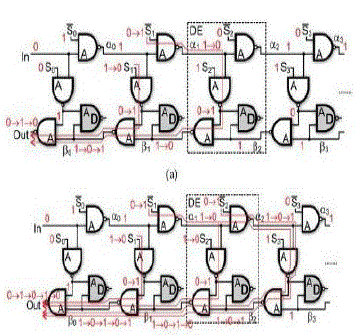
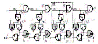
| The structure of proposed DCDL is shown in Fig. 3. In this figure “A” denotes the fast input of each NAND gate. Gates marked with “D”, represents dummy cells added for load balancing. |
 |
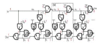 |
| According to the chosen control-bits encoding, each delayelement (DE) can be in one of three possible states. In this state the NAND “3” output is equal to 1 and the NAND “4” allows the signal propagation in the lower NAND gates chain. In this state the upper input of the DE is passed to the output of NAND “3”. The next DE (i=c+1) is in post-turn-state (Si=1,Ti=0) . In this DE the output of the NAND “4” is stuckat 1, by allowing the propagation, in the previous DE (which is in turn-state), of the output of NAND “3” through NAND “4”. All remaining DEs (for i>c+1) are again in turn-state (Si=Ti=1). The glitch-free switching property of the proposed DCDL is conceptually simple to demonstrate. After the K+1th DE switching, all cells are either in pass-state or in turn-state. In these conditions it is possible to freely change the state of DEs from pass-state to turn-state, since this change does not affect the logic state of signals. This procedure has the drawback to require a three-step switching of the DCDL. The following section provides a more detailed analysis of the glitching of proposed circuit in order to show that a glitchfree operation can also be achieved by using a properly designed two-step switching mechanism. The last signal plotted in Fig. 2 is the output of proposed DCDL of Fig. 4, simulated by using the above described three step switching mechanism, and in the same conditions of the NAND-based DCDL [12]–[15].This simulation confirms that no glitching is obtained at the output of proposed DCDL. In Fig. 3, by increasing the control code by one, two NAND gates are inserted in the signal propagation path between In and Out. The circuit of Fig. 3 is an inverting DCDL. In this circuit it is interesting to observe that the first DE is never in post-turn state,therefore T0 is always 1. This observation allows to construct a non-inverting DCDL by modifying only the first DE, as shown in Fig. 4. In this circuit the NAND gates “1” and “2” of the first DE have been deleted, together with signal T0.The signal of the second DE is now equal to In, therefore the whole behavior of the DCDL is non-inverting. The last signal plotted in Fig. 3 is the output of DCO designed by using proposed DCDL of Fig. 4. This simulation confirms that no glitching is obtained at the output and this results in a correct DCO operation. In fact the simulation shows that the DCO output switches correctly from 500 to 333 MHz and back to 500 MHz, without any glitch or any problem. |
GLITCH-FREE SWITCHING OF PROPOSED DCDL AND CONTROL-BITS DRIVING CIRCUITS |
| In the previous section we have seen that the glitch-free operation of the proposed DCDL can be obtained with a threestep switching mechanism: for a switching from a delay control code c=k to a delay control code c=h, first, the k+1th DE is switched from post-turn-state to the turn-state; next all DE are switched from pass to turn-state (or vice versa) and finally the h+1th DE is switched to post-turn-state. This switching mechanism presents the drawback of being slow and can result in a not simple driving circuit for the DCDL control-bits. |
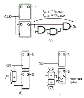 |
| Fig. 5. Possible driving circuits for the control-bits of proposed DCDL:(a)Si signals delayed with different LH/HL delays by using a NAND-based circuit; (b)Signals delayed using clock-tree delay (c)Si delayed with different LH/HL delays by using clock-tree delay and double-clock flip-flops The Fig. 5 shows three possible driving circuits that can be used to generate the control-bits of the proposed DCDL. By analyzing Fig. 6 it can be noted that Si signals have to be delayed with respect to Ti signals and that it could be useful to have a different delay for LH and HL transitions. It is also worth to note that, to avoid glitching of the DCDL, Si and Ti signals must themselves be glitch free. By following this reasoning, in all presented driving circuits, it is assumed that Ti signals are generated as output of flip-flops, which, at the same time, both properly time the DCDL considering systemlevel aspects, and act as deglitching elements. The Fig. 5(a) shows the first driving technique. In this solution each signal is obtained by using a flip-flop followed by a NAND-based circuit which presents different LH and HL propagation delays. A drawback of this solution is the relatively large complexity, since, for each signal, a driving circuit composed of three NAND gates is needed (in addition to the flip-flop). The driving circuit of Fig. 5(b) results simpler than the circuit of Fig. 5(a). In this second solution signals are delayed by delaying the clock signal of the flip-flops. The clock signal delay can be easily obtained by properly designing the clocktree. In a standard-cells design flow based on automatic place and route, a different clock-tree delay can be obtained on a flip-flop by flip-flop bases by using the useful-skew feature of the tools. The third solution of Fig. 5(c) joins the advantages of the two previous solutions. The circuit of Fig. 5(c) is based on the employ of a special flip-flop that we will name doubleclock flip-flop in the following. This flip-flop employs two different clock signals: one clock signal is used to capture the high logic-state of the D input while another clock signal captures the low logic-state of the D input. In the driving circuit of Fig. 5(c), this special flip-flop allows to control separately the LH and HL instants of switch of the signals through the delays of the two clock signals. |
SIZING AND SIMULATION RESULTS |
| In order to verify the effectiveness of proposed solution, the circuits of Figs. 1–5 and the DCDL of [8] have been designed for a 90-nmCMOS technology, with 1.0V supply voltage and using standard devices. The considered length, for all DCDLs, is 64 elements. Before to evaluate the performances of the DCDLs, a series of simulations to verify the glitching behaviour have been performed. To that purpose a simulation test-bench has been considered in which the delay controlcode is changed by using a test vector of 10 000 random delay control-codes. In these conditions, the circuit of Fig. 1 exhibited 5208 glitches. The glitchingbehavior of proposed DCDL has been verified by considering the waveforms of Fig. 4, and by varying the two delays. The Fig. 5 shows the obtained simulation results and compares these results with the two timing constraints. The graph presents on the two axis the delays, normalized to the NAND gate propagation delay. A circle and a cross are used to represent simulations in which either no glitching or a glitchingbehavior is observed, respectively. |
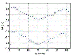 |
| The analysis of confirms the correctness of the model developed in Section IV, highlighting that effectively the two constraints (5), (6) represent a worst-case condition. The minimum delay of proposed non-inverting DCDL is very close to minimum delay of NAND-based DCDL [12]–[15]. The lowest is achieved by TINV-based DCDL [8]. This solution, however, pays a 58% higher with respect to NANDbased DCDL and a higher power dissipation. Please note that proposed DCDLs result in a lower power dissipation with respect to TINV-based DCDL [8] since transistor sizing can be much more efficient in proposed circuit with respect to TINV-based DCDL, where the PMOS sizing has to be about 2.5 times larger than nMOS. The Fig. 6 shows the simulated INL of the proposed non-inverting DCDL. |
CONCLUSION |
| A NAND-based DCDL which avoids the glitching problem of previous circuit has been presented. A timing model of the novel DCDL structure has been developed to demonstrate the glitch-free property of the proposed circuit. As an additional result, the developed model provides also the timing constraints that need to be imposed on the DCDL control-bits in order to guarantee a glitch-free operation. Three different driving circuit for the DCDL control-bits, which verify the given timing constraints, have been also proposed in the paper. The simulation results confirm the correctness of developed model and show that proposed solutions improve the resolution with respect to previous approaches. As example application proposed DCDL is used to realize an all-digital SSCG. The employ of proposed DCDL in this circuit allowed to reduce the peak-to-peak absolute output jitter of more than the 55% with respect to an SSCG using three-state inverter-based DCDLs. |