ISSN ONLINE(2319-8753)PRINT(2347-6710)
ISSN ONLINE(2319-8753)PRINT(2347-6710)
| R. Logeswaran, R. Selvamanikandan, N. Subramanian, G. Jothi Priya Department of Electrical and Electronics Engineering, Magna College of Engineering, Chennai, India |
| Related article at Pubmed, Scholar Google |
Visit for more related articles at International Journal of Innovative Research in Science, Engineering and Technology
The aim of this project is to build a compact scheme for monitoring and protecting the substation and its feeders. Presently SCADA is available only in LOAD DESPATCH CENTRES located in CHENNAI and in ERODE. The load dispatch centre is equipped with the SCADA software and the required hardware. The hardware includes the data acquisition, data processing, data transmission etc. All the substations are linked with Load dispatch centres through scada. The operator in the load dispatch centre monitors the parameters and status of any of the substation or the feeders connected to the generating stations. They are monitoring the whole power system and instructing the operators in the substation for the safe operation. They are also assisting the substation operators for the failure, disturbance and restoration
Keywords |
| Power supply unit - Schematic circuit -AC current measuring circuit-AC voltage measuring circuit- Relay driver circuit,-Interface card- c program. |
OBJECTIVES |
| The main objective of the project is to introduce scada in the substation with the help of simple hardware and graphics. C based program is to be developed to interface the user and the power system through scada computer. Mylapore 230kv/110kv substation is taken as a model for introducing scada. |
EXISTING SCHEME |
| Manual switching operation carried out from the control desk or control panel. At present no computer is used to switch on or switch off the feeder at the substation level. 220v dc or 230v ac control supply is given to the manual switching device. 220v dc or 230v ac is extended to the contactor directly or through relay when switch is operated. |
PROPOSED SYSTEM |
| To build a compact scheme for monitoring and protecting the substation and its feeders. Presently SCADA is available only in LOAD DESPATCH CENTRES located in CHENNAI and in ERODE. The load dispatch centre is equipped with the SCADA software and the required hardware. The hardware includes the data acquisition, data processing, data transmission etc. All the substations are linked with Load dispatch centres through scada. The operator in the load dispatch centre monitors the parameters and status of any of the substation or the feeders connected to the generating stations. They are monitoring the whole power system and instructing the operators in the substation for the safe operation. |
 |
HARDWARE REQUIREMENTS |
| The basic hardware design is printed circuit board for various circuits. The hardware consists of primary circuits used for giving inputs and getting outputs. Different hardware parts are designed and the circuits are developed on the PCB specially designed for their own purpose. Different PCB’s used here are shown separately. Each one of the hardware circuit is explained separately and clearly with their circuit diagrams, components used, working, purpose, etc. The PCB is designed for: |
| Power Supply Unit |
| Voltage control unit |
| Drive Circuit |
| AC Voltage transducer |
| AC current transducer |
| Analog to Digital Converter |
| Interface Circuit |
| Schematic cricuit |
FUNCTIONAL BLOCK DIAGRAM |
 |
| FIGURE2: Functional Block Diagram |
| A 230V, 50Hz AC supply is stepped down to 15V using a step down transformer. This supply is converted to DC using a bridge rectifier circuit. Two voltage regulators IC7805 and IC7812 are used to convert the 15V DC to 5V and 12V respectively. ADC and Interface, analog simulation board, binary simulation board and transducer (voltage, current, and frequency) are fed with the 5V DC supply. The drive circuits are fed with the 12V DC supply.The inputs from analog simulation board, binary board and transducer (voltage, current, frequency) are given to ADC. The printer port is connected to PC and ADC board. The PC generates commands to trigger the drive circuit via the ADC board. Based on the feeders which are switched ON/OFF can be identified. |
SCHEMATIC DIAGRAM |
 |
HARDWARE COMPONENTS |
| POWER SUPPLY UNIT |
| The term is most commonly applied to electric power converters that convert one form of electrical energy to another, though it may also refer to devices that convert another form of energy (mechanical, chemical, solar) to electrical energy. A regulated power supply is one that controls the output voltage or current to a specific value; the controlled value is held nearly constant despite variations in either load current or the voltage supplied by the power supply's energy source. Every power supply must obtain the energy it supplies to its load, as well as any energy it consumes while performing that task, from an energy source. Depending on its design, a power supply may obtain energy from Electrical energy transmission systems. Common examples of this include power supplies that convert AC line voltage to DC voltage. Energy devices such as batteries and fuel cells.Electromechanical systems such as generators and alternators.Solar power. The total power supply module consists of Step down transformer , Full Wave Rectifier, Voltage regulators/transistor, Capacitors. |
 |
| TRANSFORMER: |
| The Ac input is taken from the main supply usually of (230-240 V),50 Hz which is converted from high level AC to low level Ac i.e. using a step-down transformer to a range of 15V.The output voltage is supplied to a bridge rectifier and the ripple contained DC voltage is smoothen by a capacitor and it’s regulated by a IC’s 7812, 7805 which is the required supply for all the IC’s designed in our project. Heat sinks are provided to protect the IC’s in-case of any overload currents. A LED is provided at the output terminal for the indication of the ON/OFF state of the circuit. |
| RECTIFIER |
| D.C. voltage using one or more P-N junction diodes. The P-N junction conducts only in one direction. It conducts when forward biased while practically it does not conduct when reverse biased. Thus if an alternating voltage is applied across P-N junction diode, during positive half cycle the diode will be forward biased and will conduct successfully. While during the negative half cycle it will be reversed biased and will not conduct at all. Thus the P-N junction diode subjected to an AC voltage acts as rectifier converting alternating voltage to a pulsating DC voltage. |
 |
| Here we are using a Bridge rectifier; it’s essentially a full-wave rectifier circuit, using four diodes forming the four arms of an electrical bridge. To one diagonal of the bridge, the Ac voltage is applied through a transformer if necessary, and the rectified Dc voltage is taken from the other diagonal of the bridge. The main advantage of this circuit is that it does not require a center tap on the secondary winding of the transformer. Hence wherever possible, AC voltage can be directly applied to the bridge. |
| FILTER |
| The filter is an electronic circuit composed of capacitor, inductor or combination of both and connected between the rectifier and the load so as to convert the pulsating Dc to pure Dc. |
 |
| Figure 6:Filter |
| There are basically two types of filter circuits, |
| Capacitor input filter and Choke input filter Looking from the rectifier side, if the first element, in the filter circuit is capacitor then the filter circuit is called capacitor input filter. While if the first element is an inductor, it is called choke input filter. The choke input filter is not in use a days as inductors are bulky, expensive and consume more power. So to minimize the ripple content in the output of bridge rectifier, filter circuit are used. Here we are using a capacitor input filter. This filter uses a single capacitor connected in shunt arm i.e. in parallel with the load resistance. As the time required by the capacitor to charge is very small and it discharges very little due to large time constant, hence ripple in the output gets reduced considerably. Though the diodes conduct partly, the load current gets maintained due to the capacitor. This filter is very popularly used in practices. |
| VOLTAGE REGULATORS |
| The regulator keeps the output voltage constant irrespective of variation in supply voltage or load current. This maintenance a constant voltage against load variations and supply variation is called voltage regulator. In this power supply board we use two (+12V,+5V) voltage regulators. |
 |
| The IC 78XX is a series of 3 terminal positive regulators with fixed output voltages making them useful in a wide range of applications. It employs internal current limiting, thermal shut down and safe operating area protection, making it essentially indestructible. If adequate heat sinking is provided, they can deliver over 1A output current. Although designed primarily as fixed voltage regulators, these devices can be used with external components to obtain adjustable voltages and currents. To specify output voltage, substitute voltage values for “XX”. A common ground is required between the input and the output voltage. The input voltage must remain typically 2V above the output voltage even during the low point on the input ripple voltage. |
| Power circuit board is used to convert the 230V AC supply to required 12V and 5V DC supply which is required supply voltage for transducers, ADC and relays. 230V AC supply is given to the primary of the transformer (230V/12V). Reduced secondary voltage of the transformer is given to the full wave rectifier which converts AC to DC voltage. Rectified DC voltage is given to IC7812 to get 12V DC supply and a 5V is obtained using IC7805 from the 12V DC to avoid power dissipation. The capacitors help to maintain a constant input to the regulator and also to eliminate any high frequency pulses that could otherwise interfere with the operation of the regulator. Voltage Regulators can withstand over current drawn due to short circuits and also over heating. Reverse polarity destroys the regulator almost instantly. To avoid this possibility, diode protection is used in the power supply. |
| FEATURES |
| Output current up to 1A |
| Output voltages of 5,6,8,9,10,12,15,18,24V |
| Thermal overload protection |
| Short circuit protection |
| Output transistor safe operating area protection |
| WORKING |
| Power circuit board is used to convert the 230V AC supply to required 12V and 5V DC supply which is required supply voltage for transducers, ADC and relays. 230V AC supply is given to the primary of the transformer (230V/15V). Reduced secondary voltage of the transformer is given to the full wave rectifier which converts AC to DC voltage. Rectified DC voltage is given to IC7812 to get 12V DC supply and a 5V is obtained using IC7805 from the 12V DC to avoid power dissipation. The capacitors helps to maintain a constant input to the regulator and also to eliminate any high frequency pulses that could otherwise interfere with the operation of the regulator. Voltage Regulators can withstand over current drawn due to short circuits and also over heating. Reverse polarity destroys the regulator almost instantly. To avoid this possibility, diode protection is used in the power supply. |
| DRIVE CIRCUIT |
| A Driver is an electrical circuit used to control another circuit, such as a high power transistor. They are used to regulate current flowing through a circuit. It also used to control the other factors such as other components in the circuit. Relay is a protective device, which is used to sense the fault condition in a system, and it gives signal to the circuit breaker to open the faulty circuit, thereby protecting the elements of the system.Here relay board comprises of six relays associated with opto-isolation IC’s. Here attractive type relays are used. The power required for relay circuit is 12V D. The control signal that is given by the PC reaches relay circuit through printer port. Before that an optoisolation IC CNY – 17 is used. This is for providing isolation between PC and hardware relays.Relay circuit consists of a transistor, inductor coil with freewheeling diode as shown in the figure. As mentioned earlier, the commands from the PC are given to the relay drive circuit. The relay drive circuit consists of medium power transistor wired in the switching mode. When an input voltage of sufficient magnitude is applied to the base of the transistor, the transistor goes into saturation, turning on the relay connected at its collector terminal. A diode is used as a freewheeling element to prevent the induced voltage in the relay coil from damping the transistor when relay driver transistor is cut-off. |
 |
| WORKING |
| Drive circuit generates trip signal, which is given to circuit breaker to remove the faulty part from the circuit as soon as fault is sensed by computer.The signal from the computer is given to input of the drive circuit as binary signals (1’s and 0’s).Under normal condition the relay remains at normally open position and if the input signal is 1 then the circuit acts to generate trip signal. If the base of the transistor is provided with input signal (binary signal 1) equivalent to 5V DC, emitter is grounded and collector gains negative potential. If the computer senses the fault condition then the drive circuit forward biases the transistor and hence forming the closed path across relay supply thereby relay is activated to generate trip signal.230V AC available at the input of the relay is available at the output and it is rectified to DC voltage using diode, capacitor acts a filter and trip signal is given to circuit breaker. |
| VOLTAGE TRANSDUCER |
 |
| Figure 9: Voltage transducer |
| The step down voltage say 110 V or 230 V AC is given to the AC voltage transducer circuit. In DC voltage transducer 110 V AC is given to the FWR where it is converted into DC voltage. A capacitor of 1000 μf /25 V acts as a filter for the voltage across the output of FWR and thereby reducing the ripples. The filtered voltage is given to the preset and a resistor of 47KΩ. The 47KΩ resistor is used to reduce the voltage and the 5KΩ preset is used to set a desired output voltage for the given input. The output of the preset, which is in the range of (0 – 5V) is given to ADC. In ADC the analog voltage signal is converted to 8 bit digital signal. The 8 bit digital signal is given to computer through ADDON- CARD. In computer the 8 bit signal is compared with predefined values specified in the program. If the signal exceeds the predetermined value, computer gives a signal to drive circuit. In our project to make it suitable for all kinds of generator, we have designed a circuit consisting of two 4.7KΩ /5W resistors, 10KΩ resistor, and 110KΩ potentiometer. To employ protection for small generator of output voltage 230V, both the 4.7KΩ resistor are included in the circuit to get the voltage drop and is given to the step down transformer through 10KΩ/5W resistor, the output is tapped from 0 – 6 leads. To ensure protection for high capacity generator, the terminal voltage of the generator is tapped through the voltage transformer and stepped down to a voltage of 110V and then supplied to the circuit. In this case only one 4.7KΩ resistor comes into action and its output is given to the step down transformer through 10KΩ resistor and the output of transformer is tapped from 6 – 6 leads. The 8 bit digital signal is given to computer through ADD-ON-CARD and is compared with predefined values specified in the program. If the signal exceeds the predetermined value, computer gives a signal to drive circuit. |
| CURRENT TRANSDUCER |
| In order to safeguard generator against over current and under current faults the stator current is tapped through current transformer of ratio 1000:1. If a generator has a stator current of about 6000A then current transformer will reduce it to 6A and it is given to the current MEASURING CIRCUIT. In current MEASURING CIRCUIT there is a current transformer, which is of rating 10:1, which reduces the current further in order to make it suitable for small electrical components. The secondary of the current transformer is connected to a 4.7KΩ resistor and a capacitor acts as a filter. The output of the preset, which is in the range of (0 – 5V) is given to ADC. In ADC the analog voltage signal is converted to 8 bit digital signal. The 8 bit digital signal is given to computer through interfacing card. In computer the 8 bit signal is compared with predefined values specified in the program. If the signal exceeds the predetermined value, computer gives a signal to trip circuit. |
 |
| Figure 10:Current Transducer |
ANALOG TO DIGITAL CONVERTOR |
| The ADC 0809 data acquisition component is a monolithic CMOS device with an 8-bit analog to digital converter, 8- channel multiplexer and microprocessor compatible control logic. The 8-bit A/D converter uses the successive approximation as the conversion technique.The 8-channel multiplexer can directly access any of 8-single-ended analog signals.Easy interfacing is provided by the Latched and decoded multiplexer address inputs and latched TTL TRI STATE OUTPUTs. The ADC 0809 offers high speed, High accuracy, minimal temperature dependence, excellent long-term accuracy and repeatability and consumes minimal power. |
 |
| INTERFACING CARD |
| Interfacing card is to transfer 8-bit data from A/D converter to computer as a set of 4-bits. 74LS244 IC is used to transfer 8-bit data into serial of 4-bit data. A0-A7 is analog signal for A/D converter and after the conversion in the A/D converter, its being B0-B7 of digital data. Data B0 to B3 are transferred to computer printer port by making the G1 low and G2 high of IC 74LS244. Similarly another set of data B4-B7 is transferred by making G1 high and G2 low. Likewise the data are transferred to the computer. |
| PARALLEL PRINTER PORT |
| Parallel Printer Port has a total of 12 digital outputs and 5 digital inputs accessed via 3 consecutive 8-bit ports in the processor's I/O space. |
| 8 output pins accessed via the DATA Port |
| 5 input pins (one inverted) accessed via the STATUS Port |
| 4 output pins (three inverted) accessed via the CONTROL Port |
| The remaining 8 pins are grounded |
| The PC parallel port adapter is specifically designed to attach printers with a parallel port interface, but it can be used as a general input/output port for any device or application that matches its input/output capabilities. It has 12 TTLbuffer output points, which are latched and can be written and read under program control using the processor In or Out instruction. The adapter also has five steady-state input points that may be read using the processors in instruction. sinterrupt. This interrupt can be enabled and disabled under program control. Reset from the power-on circuit is also ORed with a program output point, allowing a device to receive a power-on reset when the processor in reset. The input/output signals are made available at the back of the adapter through a right-angled, PCB-mounted, 25-pin, D-type female connector. This connector protrudes through the rear panel of the system, where a cable may be attached. When this adapter is used to attach a printer, data or printer commands are loaded into an 8-bit, latched, output port, and the strobe line is activated, writing data to the printer. The program then may read the input ports for printer status indicating when the next character can be written, or it may use the interrupt line to indicate "not busy" to the software. These input ports are used for sending the data from the transducer to the system. |
SIMULATION RESULT |
| GRAPHICAL VIEW ON UNDER VOLTAGE OPERATION |
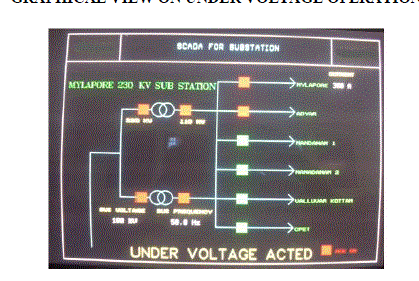 |
| Figure 12: Schematic output of under voltage operation |
| GRAPHICAL VIEW ON OVER CURRENT OPERATION |
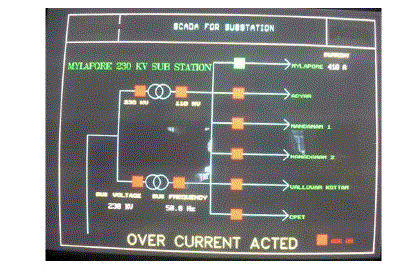 |
| Figure 13: Schematic output of over current operation |
| ADVANTAGE |
| Substation operation will be completely system oriented. |
| Improves the power system operation and reliability. |
| Ensured operation is possible. |
| Feeders can be protected against overloading. |
| Feeders also can be protected against failure due to abnormal loads for long time. |
| It helps to prevent multiple failures and avoid emergency. |
| Monitoring of a substation task may be made simple and identification of failure is very fast with the aid of scada. |
CONCLUSION |
| Implementing the SCADA in the field of substation improves the reliability, sensitivity and fault clearing time in substation and thereby improves power system stability. |
References |
|