ISSN ONLINE(2319-8753)PRINT(2347-6710)
ISSN ONLINE(2319-8753)PRINT(2347-6710)
| Vithya.T, Snekapriya.T Department of EEE, Bannari Amman Institute of Technology, Sathyamangalam, India |
| Related article at Pubmed, Scholar Google |
Visit for more related articles at International Journal of Innovative Research in Science, Engineering and Technology
This paper deals with performance analysis of PV fed single phase T-source inverter for a standalone system. The T-source inverter has an ability to perform DC to AC conversion and buck boost operation in a single stage. Compared to Z-source inverter the number of passive elements are reduced in T-network. The traditional voltage and current source inverters cannot provide such feature. Normally, the proportional integral (PI) control is commonly used in the stationary reference frame for current controlled inverters. However, it has two main drawbacks: inability to track a sinusoidal reference without steady state error and poor disturbance rejection capability. These problems are overcome by using proportional resonant (PR) controller. The performance analysis of T-source inverter is carried out with PI and PR controller. A simulation of Single phase T-source inverter is done using MATLAB/ Simulink.
Index term |
| Photovoltaic (PV) cell, T-source inverter, Proportional Resonant (PR) controller, Simple boost control |
INTRODUCTION |
| Power electronic converter system plays an important role in the integration of photovoltaic (PV) sources into the load. Today, a distribution configuration of single-phase grid connected PV inverters with high efficiency, high reliability, and reasonable cost is possible [1]. A PV cell is an electronic device which directly converts sunlight into electricity. Light shining on the solar cell produces both a current and a voltage to generate electric power. The output dc voltage is converted into ac by inverters. The z-source inverter was introduced by F.Z.Peng. This Z-source inverter overcomes the difficulties of conventional voltage and current source inverters. It performs both buck and boost operation. It can be used for both voltage and current source inverter without changing the circuit design also improves the efficiency of the system because of power conversion stage in this circuit is reduced. By modifying the arrangement of passive components we can improve the inverter performance. Among different topologies of Zsource inverter, the topology that is being considered for analysis is T-source inverter. The passive component arrangement is look like the alphabet T. The name of Tsource inverter is modified Z-source inverter. As the inverter is derived from the root of Z.-source inverter and the arrangement of passive components looks like the alphabet ‘T’, the inverter is called modified Z-source inverter or T-source inverter. The boost operation of the inverter is achieved using the concept of shoot-through time period. Normally the current control scheme is used in single phase photovoltaic inverter. It consists of tracking regulator with proportional Integrator compensator. But it introduces steady state error in amplitude and phase. Although we can attenuate steady state error by increasing the control gain, it also increases the system instability and noise. As an alternative approach, tracking regulators with a proportional-resonant (PR) compensator have been presented. The resonant term behaves a generalized integrator (i.e., an integrator for a sinusoidal signal) and is composed of a second order band pass filter tuned to resonant at the grid frequency. PR controller introduces the infinite gain at resonant frequency. With the PR compensator, the grid current can perfectly track the reference signal with zero steady state error. Moreover the generalized integrator has a negligible effect on inverter noise and stability due low band width to the band pass filter. The common problem is load voltage distortion introduce harmonic components in the current. This problem is overcome by adding the harmonic compensator with PR controller. |
T-SOURCE INVERTER |
| The New type T – source inverter (TSI) overcome the limitation of traditional voltage source inverter and current source inverter [6] [7]. With the use of TSI, the inversion and also the boost function are accomplished in a single stage. TSI has fewer components. Due to these reasons, the efficiency appreciably increases. Unlike the traditional inverter, TSI utilizes a unique impedance network that links the inverter main circuit to the DC source. The passive element of inductor and capacitor is reduced in Tsource inverter (TSI). The two inductors are building together and it forms a couple inductors and it has low leakage inductance. Instead of two capacitors used in Zsource inverter (ZSI) the only one capacitor is used in Tsource inverter. It should be made with high precision. TSI has the feature of the common dc rail used between source and inverter. The transformer ratio must be 1:1 ratio. The impedance network output is applied to the inverter circuit and the inverter circuit consists of four switches. Boosting capability is achieved by shoot through mode of switches operation. This operation performed by turning on the both switches simultaneously[13]. |
 |
| Figure 1: Circuit Diagram of New Type T – Source Inverter |
| During the shoot through mode state the energy is transferred from capacitor to inductor. At the time, the voltage boosting is capability achieved. The DC voltage is fed as input to the impedance network of TSI which helps to achieve voltage buck and boost properties. Since, the capacitors may be charged to higher voltages than the source voltage, the diode ‘D’ prevents discharging of capacitors through the source. |
| 2.1 Modes of operation: |
| T – Source Inverter operating principle same as that of conventional ZSI [2]. The T-network is used instead of the LC-network for boosting the output voltage by inserting shoot through states in the PWM. TSI operate in two modes: a) Shoot through mode b) Non shoot through mode |
| A.Shoot through mode: |
| Fig 2. Shows the equivalent circuit of T – Source Inverter in Shoot through mode operation. This shoot through zero state prohibited in traditional voltage source inverter. It can be obtained in three different ways such as shoot through via any one phase leg or combination of two phase leg. During this mode, Diode is reverse biased, separating DC link from AC line. |
 |
| Figure 2: Shoot-through mode |
| B.Non – shoot through mode: |
| Fig 3. Shows the equivalent circuit of TSI in Non – shoot through mode operation. In this mode, the inverter bridge operates in one of traditional active states, thus acting as a current source when viewed from T – source circuit. During active state, the voltage impressed across the load. The diodes conduct and carry current difference between the inductor current and input DC current. Note that both the inductors have an identical current because of coupled inductors. |
 |
| Figure 3: Non shoot-through mode |
| During the design of TSI the most challenging is the estimation of values of the reactive components of the impedance network. The component values should be evaluated for the minimum input voltage of the converter, where the boost factor and the current stresses of the components become maximal. Calculation of the average current of an inductor |
 (1) (1) |
| The maximum current through the inductor occurs when the maximum shoot-through happens, which causes maximum ripple current. In our design, 60% peak-to-peak current ripple through the Z-source inductor during maximum power operation was chosen. Therefore, the allowed ripple current is ΔIL, and the maximum current through the inductor is ILmax: |
 (2) (2) |
| The boost factor of the input voltage is: |
 (3) (3) |
| Where D0 is the shoot-through duty cycle: |
 |
| Calculation of required inductance of Z-source inductors: |
 (4) (4) |
| where T0 - is the shoot-through period per switching cycle Calculation of required capacitance of Z-source capacitors: |
 (5) (5) |
 |
| Figure 4: Equivalent circuit of photovoltaic model |
MODELING OF PV MODULE |
| The use of equivalent electric circuits makes it possible to model characteristics of a PV cell. The method used here is implemented in MATLAB. The same modeling technique is also applicable for modeling a PV module [3]. |
| The photon generated current will follow out of the cell as a short-circuit current (Isc). Thus, |
| The output current (I) from the PV cell is found by applying the Kirchhoff’s current law (KCL) on the equivalent circuit shown in Fig 4 |
 (6) (6) |
| Where, Isc is the short-circuit current that is equal to the |
| Photon generated current |
| Id is the current shunted through the intrinsic diode. |
| Vd is the voltage across the diode (V) |
| RP is Parallel Resistance (ohm) |
| The diode current Id is given by the Shockley’s diode equation: |
 (7) (7) |
| Where: Io is the reverse saturation current of diode (A), |
| q is the electron charge (1.602×10⁻¹⁹ C), |
| Vd is the voltage across the diode (V), |
| k is the Boltzmann’s constant (1.381×10⁻²³ J/K), |
| T is the junction temperature in Kelvin (K). |
| Applying the Kirchoff’s voltage law (KVL) on the equivalent circuit |
 (8) (8) |
| Replacing Id of the equation (6) by the equation (7) gives the current-voltage relationship of the PV cell |
 (9) (9) |
| Where V is the voltage across the PV cell I is the output current from the cell The reverse saturation current of the diode (Io) is constant under the constant temperature and found by setting the open-circuit condition. Using the equation (9), let I = 0 (no output current) and solves for Io. |
 (10) (10) |
| To a very good approximation, the photon generated current, which is equal to Isc, is directly proportional to the irradiance, the intensity of illumination, to PV cell. Thus, if the value, Isc, is known from the data sheet, under the standard test condition, Go=1000W/m2 at the air mass (AM) = 1.5, then the photon generated current at any other irradiance, G (W/m2), is given by: |
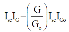 (11) (11) |
| The PV cell output is both limited by the cell current and the cell voltage, and it can only produce a power with any combinations of current and voltage on the I-V curve. It also shows that the cell current is proportional to the irradiance[12]. |
SIMPLE BOOST CONTROL |
| Fig 5. Shows the block diagram of the simple boost control (SBC) technique. In simple boost control, the reference signal is compared with the triangular carrier signal for generating the shoot through pulses (with equal or greater than the peak of triangular signal). To produce switching pulses, two reference waveform having peak value with modulation index (M) are compared with the same triangular frequency triangular signal [5]. These two signals compared by using comparator. By using logic gate, the shoots through pulses are inserted into the switching waveform. These pulses are given to the power IGBT through isolation and gate drive circuit. |
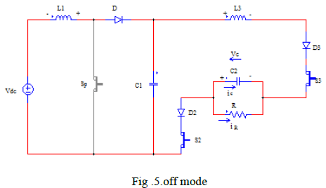 |
| Figure 5. Block diagram of simple boost control |
| Major expressions of SBC method are outlined here, |
| Modulation index: |
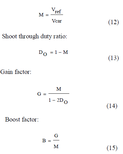 |
| The high voltage gain and a small modulation index have to be used for produce the output voltage. The voltage stress across the switches is high by using this control method. This will restrict the obtainable voltage gain because of the limitation of device voltage rating. |
PR CONTROLLER |
| This chapter will focus on the inverter control scheme. The harmonic distortion level in conventional solar power is reduced by proportional integrator controller. But, it has two main drawbacks: inability to track a sinusoidal reference without steady-state error and poor disturbance rejection capability. In order to eliminate these problems, a proportional plus resonance (PR) controller can be used. The PR controller is a double integrator that has an infinite gain at a certain frequency and almost no attenuation outside this frequency. Therefore, the PR controller can be used as a notch filter to compensate the harmonics in a very selective way. |
| In the conventional load side inverter system, an L filter was used to interface with the load. To improve the attenuation ability for high frequencies, the L filter was replaced by an LCL filter, and a damping resistor was added to improve the stability of the filter. If the rated power of the system is large, the power loss on the damping resistor is also large. In the conventional control, all control parameters were calculated in the synchronous frame which is complex, while the control scheme proposed in this chapter calculates the parameters in the stationary frame which is easier and more accurate. Although the new control scheme needs one more current sensor than the conventional scheme, when the rated power goes high, comparing the reduction of the power loss and the cost of the sensor, this scheme becomes practical and economical. |
| 5.1 Conventional PI controller |
| Current regulation is an important issue for power electronic converters and inverter. Over the last few decades, much research has been done in this area for voltage source inverters. A PI controller is commonly used for a fixed switch frequency. Proportional-integral (PI) control is commonly used in the stationary reference frame for current controlled inverters. However, this solution has two main drawbacks: inability to track a sinusoidal reference without steady state error and poor disturbance rejection capability [8][11]. |
| 5.2 PR controller design |
| Single-phase inverters are commonly used in applications like residential (typically PV or fuel cell systems) and UPS. The reference current outputs of the outer loops dc link current and reference current are next tracked by an inner current loop whose output is eventually fed to a PWM modulator for switching the inverter. |
| Typically, the inner current loop is implemented using a stationary PI current controller with voltage feed forward. Using PI control, however, leads to steady-state current error (both in phase and magnitude) when tracking sinusoidal input, and hence a poor harmonic compensation performance is expected. PI control can mitigate the tracking error, but is generally difficult to apply. Instead, the equivalent stationary PR controller can be used as the inner current controller[10], as shown in Fig 6. Compared to a stationary PI controller, the only computational requirement imposed by the PR controller is an extra integrator for implementing a second order system. Using a PR controller would allow the removal of the grid voltage feed forward path and the simple cascading of a HC compensator for eliminating selected low-order [8] [9]. |
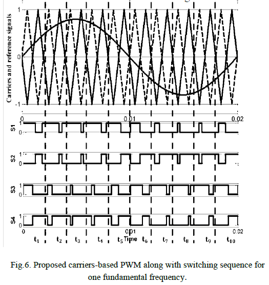 |
| Figure shows the detailed picture of the standard control scheme for single phase T-source inverter. The tracking regulator of the standard control scheme is based on a PR compensator. |
| Where Kp is the proportional gain and H1(s) which is generalized integrator, is a band pass filter tuned to resonant at the system frequency f0. That is, |
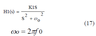 |
| The resonant harmonic compensator, which is connected in parallel with the tracking regulator, is formed by several band pass filters tuned to resonant at the desired harmonic frequency |
 |
| Where n taken the values 3,5,…..,h (with h being the highest current harmonic to be attenuated) |
SIMULATION RESULTS |
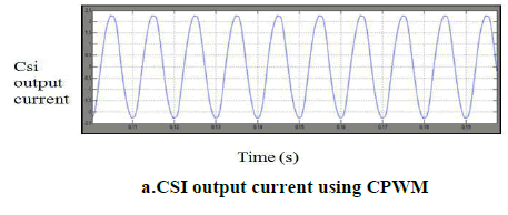
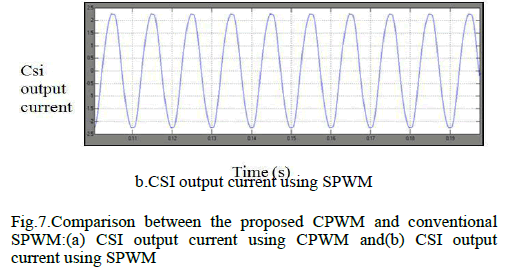
| The input voltage is 100V. The output voltage is boosted Up to 180V by performing shoot-through operation in Tsource inverter. Fig 8 shows the output voltage of TSI with filter |
 |
 |
| Fig 11. Shows The Proposed Method Output THD Of TSource Inverter Using SBC With PR Controller. Comparing To PI Controller The Proportional Resonant Controller Reduce The Lower Order Harmonic Level Of 5th And 7th. |
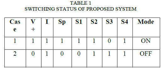 |
| Table I. Comparison of PI and PR Controller |
CONCLUSION |
| This paper has been investigated the performance of single phase T-source inverter with PI and PR controller. The voltage boost is inversely related to the shoot through duty ratio-source TSI has fewer reactive components when compared to ZSI and both the buck-boost operation is performed. The single phase TSI with PR control scheme was simulated and the lower order harmonics in the output current was reduced. |
References |
|