International Journal of Innovative Research in Science, Engineering and Technology
ISSN ONLINE(2319-8753)PRINT(2347-6710)
ISSN ONLINE(2319-8753)PRINT(2347-6710)
| SHUBHANGI V. PATIL1, TEJASHREE R. SHUKLA2, PARESH J. SHAH3 M.E. SCHOLAR, DEPARTMENT OF ELECTRONICS AND TELECOMMUNICATION, SSBTS COLLEGE OF ENGINEERING AND TECHNOLOGY,BAMBHORI, JALGAON, INDIA1 M.E. SCHOLAR, DEPARTMENT OF ELECTRONICS AND TELECOMMUNICATION, SSBTS COLLEGE OF ENGINEERING AND TECHNOLOGY,BAMBHORI, JALGAON, INDIA 2 ASSOCIATE PROFESSOR, DEPARTMENT OF ELECTRONICS AND TELECOMMUNICATION, SSBTS COLLEGE OF ENGINEERING AND TECHNOLOGY, BAMBHORI, JALGAON, INDIA3 |
| Related article at Pubmed, Scholar Google |
Visit for more related articles at International Journal of Innovative Research in Science, Engineering and Technology
This paper presents a proportional integral derivative (PID) controller model for buck converter topology of switch mode power supply (SMPS). PID controller in terms of the settling time while exhibiting a greater degree of robustness regarding disturbance rejection represented by severe changes in static and dynamic loads. The controller is used to change the duty cycle of the converter and thereby, the voltage is regulated. The buck converter, P, PI and PID controller are modeled and are evaluated by computer simulations. It has been found that the transient performance and steady state performance is improved using PID controller. SMPS design can produce very compact and lightweight supplies. Power conversion efficiencies of SMPS are 70 & 80 %. Implementation of SMPS by using FPGA, it gives the better performance and faster transient response. Improves the steady state performance and transient response by using PID controller, it is possible to design stable, efficient and ruggedized SMPS which has faster transient response for dynamically switching loads. In SMPS the switching action means the series regulator element is either on or off and therefore little energy is dissipated as heat and very high efficiency levels can be achieved. As a result of the high efficiency and low levels of heat dissipation, the switch mode power supplies can be made more compact. Switch mode power supply technology can be sued to provide high efficiency voltage conversions in voltage step up or boost applications or step down buck applications.
Keywords |
||||||||||||||||||||
| buck converter, dc-dc power conversion, proportional integral derivative (PID), control systems and field programmable gate arrays (FPGA). | ||||||||||||||||||||
INTRODUCTION |
||||||||||||||||||||
| SMPS design can produce very compact and light weight supplies. Furthermore, by employing high switching frequencies, the sizes of the power transformer and associated filtering components in the SMPS are dramatically reduced in comparison to the linear. For example, an SMPS operating at 20 kHz produces a 4 times reduction in component size, and this increases to about 8 times at 100 kHz and above. This means an SMPS design can produce very compact and lightweight supplies. This is now an essential requirement for the majority of electronic systems. We have to use the DC to DC buck Converter topology to implement the SMPS. These are the simplest configurations possible, and have the lowest component count, requiring only one inductor, capacitor, transistor and diode to generate their single output. DC-DC converters efficiently convert an unregulated DC input voltage into a regulated DC output voltage. Compared to linear power supplies, switching power supplies provide much more efficiency and power density. Switching power supplies employ solid-state devices such as transistors and diodes to operate as a switch: either completely on or completely off. Energy storage elements, including capacitors and inductors, are used for energy transfer and work as a low-pass filter [5]. Buck converter is used to convert unregulated dc input to a controlled dc output with a desired voltage level. Together with buck is PID controller that uses to control the behaviors of the system in linear. This system is a close loop system with feedback. | ||||||||||||||||||||
| A PID controller is a generic control loop feedback mechanism widely used in industrial control systems. A PID controller attempts to correct the error between a measured process variable and a desired set point by calculating and then outputting a corrective action that can adjust the process accordingly [4]. The PID controller calculation (algorithm) involves three separate parameters; the proportional, the integral and derivative values. The proportional value determines the reaction to the current error, the integral determines the reaction based on the sum of recent errors and the derivative determines the reaction to the rate at which the error has been changing. The weighted sum of these three actions is used to adjust the process via a control element such as the position of a control valve or the power supply of a heating element. By tuning the three constants in the PID controller algorithm the PID can provide control action designed for specific process requirements. The response of the controller can be described in terms of the responsiveness of the controller to an error, the degree to which the controller overshoots the set point and the degree of system oscillation. Note that the use of the PID algorithm for control does not guarantee optimal control of the system [4]. | ||||||||||||||||||||
| Digital PID control algorithm is simple because of its good robustness and high reliability, widely used in DC/DC converters digital control areas. Currently, the number of PID parameters, often through trial and error tuning, time-consuming, and poor control performance, adaptability is poor. It has long been seeking a more efficient digital PID parameter tuning methods. | ||||||||||||||||||||
| Pulse width modulation (PWM) is the main part in designing a buck converter. By using PWM control, regulation of output voltage is achieved by varying the duty cycle of the switch. Duty cycle refers to ratio of the period where power semiconductor is kept ON to the cycle period. PWM is a powerful technique for controlling analog circuits with a processor's digital outputs [4]. PWM is employed in a wide variety of applications, ranging from measurement and communications to power control and conversion. Control of PWM is usually affected by an IC is necessary for regulating the output. The transistor switch is the most important thing of the switched supply and controls the power supplied to the load. It is also stated that Power MOSFET’s. Choosing of transistor also must consider its fast switching times and able to withstand the voltage spikes produced by the inductor [4]. | ||||||||||||||||||||
| This is presented the design of a classic PID control and a digital pulse width modulator (DPWM) as the main module for a buck converter. Buck converter is controlled through a high-bandwidth multi sampled digitally controller using ripple compensation. The multisampling techniques reduce the PWM phase lag, ultimately breaking the bandwidth limitation. The proposed control is a feedback technique and needs no preliminary knowledge of converter parameters [1]. PID controllers are used in more than 95% of closed-loop industrial processes. It can be tuned by operators without extensive background in Controls, unlike many other modern controllers that are much more complex but often provide only marginal improvement. In fact, most PID controllers are tuned on-site [1]. | ||||||||||||||||||||
| With regard to robust controllers implemented on a FPGA, for the regulation of the output voltage of the buck converter, the study in [17] presents a comparison between two PID average controllers. In the recent years, technology advances in very-large-scale integration (VLSI) have made digital control of DC-DC converters. FPGA-based digital PID controller is proposed because the operations on FPGA are hardware compatible operations. However, FPGA-based digital PID controller still needs multipliers for computation. These multipliers will decrease the speed of processing time because the multiplying stage is a consumption process which introduces propagation delay and uses large part of silicon area. FPGAs provide an attractive architecture for power electronics control systems due to their ability to produce custom high-frequency, low-latency (ns) gating signals, ability to place DPWM and dead-time circuits in dedicated hardware, high speed true-parallel digital signal processing capabilities, and silicon-gate-level (SGL)user configurability. Due to the fast changing requirements of the smart grid and renewable energy markets, the inherent field re-configurability of FPGAs is also attractive from the perspective of long-term support, maintenance and interoperability with evolving standards and communication protocols. | ||||||||||||||||||||
| The lowest cost FPGAs on the market have now reached the $5 range in high-volume, which makes them attractive not only for proof-of-concept research prototypes but also for mass-produced converters. While FPGAs have been the dominant control platform for research in high-frequency, low-power SMPS in the last decade, industry development teams have been challenged to incorporate FPGAs as the main processing unit for a number of reasons [9]. First, FPGA development remains outside the reach of many skilled power electronics designers, since it requires register-transfer-level (RTL) programming methods, such as Verilog and VHDL. | ||||||||||||||||||||
II. DC –DC BUCK CONVERTER USING PID CONTROLLER |
||||||||||||||||||||
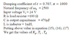
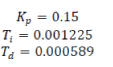
| Fig. 1 shows the block diagram of the FPGA-based SMPS using DC-DC Buck Converter based on the PID controller. The parameter values for the “buck” converter and the specifications were given in the previous section. The values of the design coefficients used by the PI and PID controllers were obtained based on the design requirements given in the previous section. The only external hardware connected to the FPGA in measuring the “buck” converter output voltage was an ADC (ADC0820) [1]. Fig.1 shows the block diagram of the FPGA-based control system based on the PID controller. | ||||||||||||||||||||
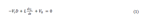
| Applying Kirchoff”s voltage law to the buck converter circuit as shown in fig. 2 | ||||||||||||||||||||
 |
||||||||||||||||||||
| Where ???? is input voltage of buck converter | ||||||||||||||||||||
| D is duty cycle for which MOSFET is ON | ||||||||||||||||||||
| L is value of inductor | ||||||||||||||||||||
| iL is current flowing through inductor | ||||||||||||||||||||
| V0 is output voltage of buck converter | ||||||||||||||||||||
| Applying Laplace transform to equation (1) | ||||||||||||||||||||
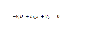 (2) (2) |
||||||||||||||||||||
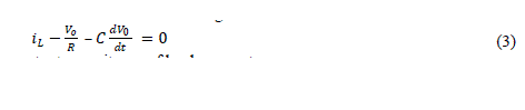
| Applying Kirchoff”s current law to the buck converter circuit shown in fig.1 | ||||||||||||||||||||
| Where R is load resistor of buck converter and C is output capacitance of buck converter | ||||||||||||||||||||
| Using Laplace transform for above equation (3) and rearranging terms for iL so that we can replace it in equation (2) | ||||||||||||||||||||
 |
||||||||||||||||||||
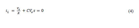
| Where R is load resistor of buck converter and C is output capacitance of buck converter | ||||||||||||||||||||
| Using Laplace transform for above equation (3) and rearranging terms for iL so that we can replace it in equation (2) | ||||||||||||||||||||
 |
||||||||||||||||||||
| Using value of iL from above equation (4) into equation (2) | ||||||||||||||||||||
 |
||||||||||||||||||||
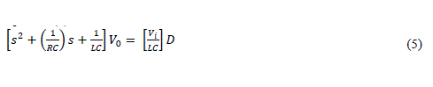
| Where D is duty cycle of PWM signal of buck converter which is output of our PID controller model of buck converter and output voltage V0 is used as input of model, hence transfer function can be written as | ||||||||||||||||||||
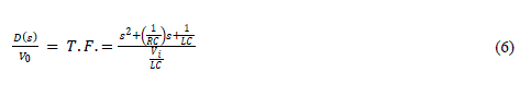 |
||||||||||||||||||||
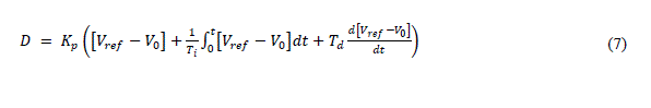
| Similarly equation of PID controller is | ||||||||||||||||||||
 |
||||||||||||||||||||
 |
||||||||||||||||||||
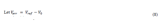
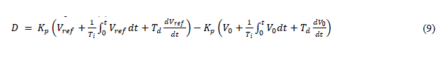
| Separating terms of Vref and V0 in equation (7) | ||||||||||||||||||||
 |
||||||||||||||||||||
| Solving terms in equation (9) | ||||||||||||||||||||
 |
||||||||||||||||||||
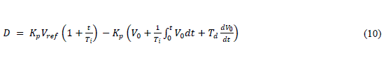
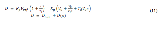
| Term containing Vref is constant part of PWM duty cycle and duty cycle of PWM signal will vary as per change in Vo Taking Laplace transform of equation (10) | ||||||||||||||||||||
 |
||||||||||||||||||||
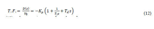
| Transfer function of PID controller is- | ||||||||||||||||||||
 |
||||||||||||||||||||
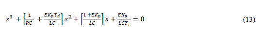
| Equating RHS of equation (6) and equation (12) and rearranging terms for orders of s | ||||||||||||||||||||
 |
||||||||||||||||||||
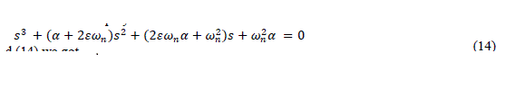
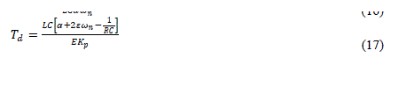
| The equation (12) becomes is of Third order Hurwitz polynomial form | ||||||||||||||||||||
 |
||||||||||||||||||||
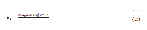
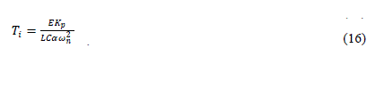
| Equating orders of equation (13) and (14) we got | ||||||||||||||||||||
 |
||||||||||||||||||||
 |
||||||||||||||||||||
 |
||||||||||||||||||||
 |
||||||||||||||||||||
 |
||||||||||||||||||||
| B. IMPLEMENTATION OF PID CONTROLLER MODEL | ||||||||||||||||||||
| PID controller equations need to be converted in discrete format so that it can be simulated and implemented. Considering equation (7) | ||||||||||||||||||||
 |
||||||||||||||||||||
| Equating equation (7) and (18) and getting following equation (separating proportional, integral and derivative parts) | ||||||||||||||||||||
 |
||||||||||||||||||||
 |
||||||||||||||||||||
 |
||||||||||||||||||||
 |
||||||||||||||||||||
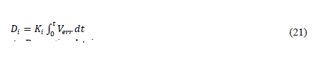
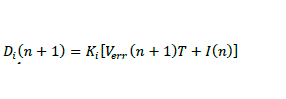
| Integral is defined by | ||||||||||||||||||||
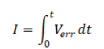 |
||||||||||||||||||||
| Its discrete approximation is defined as | ||||||||||||||||||||
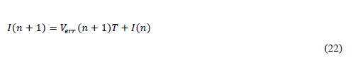 |
||||||||||||||||||||
 |
||||||||||||||||||||
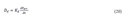
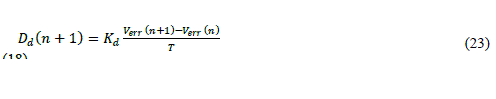
| Discrete approximation of derivative is defined as | ||||||||||||||||||||
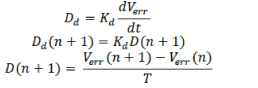 |
||||||||||||||||||||
 |
||||||||||||||||||||
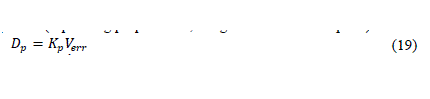
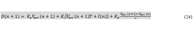
| Putting equation (19), (22), (23) in equation (18) | ||||||||||||||||||||
 |
||||||||||||||||||||
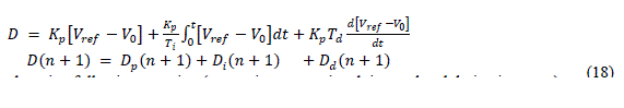
| Above equation is used to implement PID controller model of buck converter topology of SMPS, here Verr acts as feedback for duty cycle calculation. | ||||||||||||||||||||
| C. SIMULATION RESULTS OF BUCK CONVERTER | ||||||||||||||||||||
| Below mentioned Fig.3 shows transient response of buck converter model, output voltage is set at 18 V, output slowly reaches to 18 V (just within 6 ms) which is reference voltage and error is difference of output voltage and reference voltage. | ||||||||||||||||||||
| Fig. 4 shows response of model when it is subjected to dip in a voltage because of sudden change in load model restores output voltage within 4 ms and also avoids overshoots in output i.e. increments duty cycle of PWM signal gradually. Similar results were found for voltage rise as well. | ||||||||||||||||||||
III. FPGA MODEL OF BUCK CONVERTER |
||||||||||||||||||||
| The basic VHDL module is an introduction to the VHSIC hardware description language and its fundamental concepts. VHDL is a language specifically developed to describe digital electronic hardware and its attributes. VHDL is a flexible language and can be applied to many different design situations. This language has several key advantages, including technology independence and a standard language for communication. The module describes many of the advantages of using VHDL and a short history of the language. This section of the paper deals with FPGA Module for dc-dc Buck converter. Here discussed the FPGA and their logic block. Also shows the Technology schematic view using Spartan 3 family of XC3S400 FPGA and PQ 208 packages. Simulation results of PID controller, PWM signal dc- dc buck converter. | ||||||||||||||||||||
| A. PID CONTROLLER | ||||||||||||||||||||
| Table1 show the Device utilization summary. This is the synthesis report. Here logic utilization is used. Like 22 number of slices is used and its utilization is 0.61%, numbers of slices flip flop is 23 and utilization is 0.32%, 4 input look up tables is 23and utilization is 0.32%, bonded input output block is 18 and utilization is 12.7%, numbers of multipliers is 2 and utilization is 12.5% and numbers of GCLKs is 1 and utilization is 12.5%. | ||||||||||||||||||||
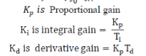
| Output of the PID controller is PWM signal here K1 = Kp + Ki + Kd , K2 = –Kp-2Kd, k3 = Kd. Kp is proportional gain, Ki is the integral gain, Kd is the derivative gain. Input of the PID controller is the e_in clk signal & reset. u_out is the output of the PID controller. Kp is use to reduced the rise time, to decrease the rise time. Ki is use to eliminate the steadystate error, Kd use to reduce the overshoot and settling time. | ||||||||||||||||||||
| Fig. 5 shows the technology schematic view of PID controller by using Spartan 3 family of XC3S400 and PQ 208 package of FPGA. In this view get look up table, truth table and K map. | ||||||||||||||||||||
| Fig. 6 shows the simulation result of PID controller. PID controller gives the faster transient response and better performance. Improve the steady state performance and transient performance.Using PID controller. | ||||||||||||||||||||
| B. PWM MODEL | ||||||||||||||||||||
| A single up–down counter unit and one comparator unit are used to create the PWM signal required to drive the buck converter. The maximum count value of the counter, in conjunction with the speed of the clock used to drive the counter, determines the PWM period frequency. The counter counts from zero to its maximum value and then from its maximum value to zero. The period of the PWM is measured from zero point to zero point in the counter cycle. The compare unit compares the count value from the counter unit with the PID controller output value. | ||||||||||||||||||||
| Table 2 show the Device utilization summary. Here logic utilization is used. Like 9 number of slices is used and its utilization is 0.25%, numbers of slices flip flop is 9 and utilization is 0.12%, 4 input look up tables is 18 and utilization is 0.25%, bonded input output block is 11 and utilization is 7.80%, and numbers of GCLKs is 1 and utilization is 12.5%. | ||||||||||||||||||||
| Fig. 7 shows the technology schematic view of PWM signal by using Spartan 3 family of XC3S400 and PQ 208 package of FPGA. In this view get look up table, truth table and K map. In this technology schematic PWM is a powerful technique for controlling analog circuits with a processor’s digital outputs. In this block A, clk and reset are the input of PWM signal and PWM is the output. To generate PWM signal the comparator and counter is used. | ||||||||||||||||||||
| Fig. 8 shows the simulation result of PWM signal by using the FPGA. Get the PWM signal and also get the duty cycle of PWM signal, period and offset time. Duty cycle refers to ratio of the period where power semiconductor is kept ON to the cycle period. | ||||||||||||||||||||
| C. DC-DC BUCK CONVERTER | ||||||||||||||||||||
| Table 3 show the Device utilization summary. Here logic utilization is used. Like 34 number of slices is used and its utilization is 0.94%, numbers of slices flip flop is 40 and utilization is 0.55%, 4 input look up tables is 49and utilization is 0.68%, bonded input output block is 21 and utilization is 14.8%, numbers of multipliers is 2 and utilization is 12.5% and numbers of GCLKs is 2 and utilization is 25%. | ||||||||||||||||||||
| Fig. 9 shows the technology schematic view of dc-dc buck converter by using Spartan 3 family of XC3S400 and PQ 208 package of FPGA. In this view get look up table, truth table and K map. In this block err is a 8 bit ,clk input of PWM, reset input of PID, reset input of PWM is the input of dc-dc buck converter. Clk output of PID, pwm_o is the output of buck converter and pid_out is the output of PID controller. | ||||||||||||||||||||
| Fig. 10 shows the simulation result of buck converter. We get the clk output of PID, output of buck converter in the form of PWM. Also get duty cycle of PWM. Get the Period and offset time. | ||||||||||||||||||||
IV. CONCLUSION |
||||||||||||||||||||
| In this paper, the PID control scheme is applied for output voltage regulation in a dc-dc buck converter. The performance of the PID control action was compared under several load conditions. Above results shows that using PID controller, it is possible to design stable, efficient and ruggedized buck converter which has faster transient response for dynamically switching loads. PID controller has a better transient response than that achieved with control action. When connect static and dynamic loads to the buck converter output, observed that the PID control results in a significantly faster response that obtained with regard to the output voltage recovery time to the desired reference. By using PID control action can be used to design switched-mode power supplies with efficiency greater than 90%. | ||||||||||||||||||||
| Digital SMPS using PID controller model can remove the disadvantages of analog SMPS, like noise, transient spikes by using PWM techniques. Digital SMPS can provide numerous advantages for low power applications like robustness, flexibility & IP reuse and the very compact and lightweight supplies and reduce the cost. In digital SMPS the switching action means the series regulator element is either on or off and therefore little energy is dissipated as heat and very high efficiency levels can be achieved. | ||||||||||||||||||||
ACKNOWLEDGMENT |
||||||||||||||||||||
| First of all, I would like to thanks my guide Prof. P. J. Shah at department of Electronic and Telecommunication of Shram Sadhana Bombay Trust’s College of Engineering and Technology, Jalgaon, Maharashtra for guidance during my work and for reading and comments on the manuscript of this thesis. The work described in this paper was supported by a research laboratory and digital library provided by SSBT COET, Jalgaon, Maharashtra. Finally, I would like to thank my husband and my family for supporting me. | ||||||||||||||||||||
Tables at a glance |
||||||||||||||||||||
|
||||||||||||||||||||
Figures at a glance |
||||||||||||||||||||
|
||||||||||||||||||||
References |
||||||||||||||||||||
|


