International Journal of Innovative Research in Science, Engineering and Technology
ISSN ONLINE(2319-8753)PRINT(2347-6710)
ISSN ONLINE(2319-8753)PRINT(2347-6710)
Mahesh Gowda N M1, Yadu Kiran2, Dr. S.S Parthasarthy3
|
| Related article at Pubmed, Scholar Google |
Visit for more related articles at International Journal of Innovative Research in Science, Engineering and Technology
In this paper, a mathematical model of a Buck Converter for simulation using Simulink without any Sim Power System Elements is illustrated. We also explain how to use Matlab’s Tuning tools to obtain better rise time, settling time and peak overshoot.
Keywords |
| Buck converter, Transfer function, PID controller, Pulse Width Modulation (PWM), Duty Cycle,Matlab, Simulink. |
I. INTRODUCTION |
| Switched mode DC-DC converters are some of the simplest power electronic circuits which convert one level of electrical voltage into another level by switching action. These converters have received an increasing deal of interest in many areas. This is due to their wide applications like power supplies for personal computers, office equipment, appliance control, telecommunication equipment, DC motor drives, automotive, aircraft, etc. The analysis, design, control and stabilization of switching converters are the main factors that need to be considered [1]. Many control methods are used for control of switch mode DC-DC converters and the simple and low cost controller structure is always in demand for most industrial and high performance applications [2]. Each control method has its own advantages and drawbacks, and its effectiveness is determined by the application where it’s applied. |
| Whether it is for designing your own product or just experimenting with various algorithms and designs, simulation runs are mandatory before the actual physical implementation. Various tools are available for constructing and simulating electrical and electronic circuits, including Math Works SimPowerSystems. However, some might not have access to these Tools and Suites. It is possible to circumvent this by representing the system in the form of a mathematical model. Therefore, in this paper we illustrate how to model a Buck Converter using the most rudimentary blocks of Simulink, while still providing the same degree of accuracy as other tools. This paper explains the working of the model and each of its subsystems. |
| In section III, a brief overview of the operation of a typical DC-DC Buck Converter is provided. Section IV proceeds to explain the Simulink model of the Buck Converter and its various subsystems. In Section V, details of a simulation run and its results are discussed. In Section VI, we give our closing comments. |
II RELATED WORK |
| Several control strategies and mathematical models have been developed by researches. Tobias Geyer, GeorgiosPapafotiou, and Roberto Frasca have proposed a modeling and control approachfor fixed frequency switchmode DC-DC converters by formulatinga constrained optimal control problem using hybrid systemsmethodologies [2].Ned Mohan, W.P. Robbins, T.M.Undeland, R. Nilssen and Olive Mo were among the first to present means of simulating Power Electronics and Motion Control systems [6]. Great strides have been made to incorporate soft computing techniques such as Fuzzy Logic, Genetic Algorithm etc, into the control strategies as well. There are also numerous publications on tuning methods of a PID controller for a Buck Converter. |
III.PRINCIPLE OF OPERATION OF A BUCK CONVERTER |
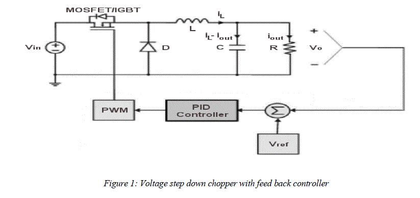 |
| Figure 1 shows the circuit configuration of the voltage step down chopper which converts unregulated DC to regulated DC.The chopper is operated by turning the MOSFET ON and OFF at a high switching frequency. Figure 2 shows the output voltage and current waveforms of the chopper. |
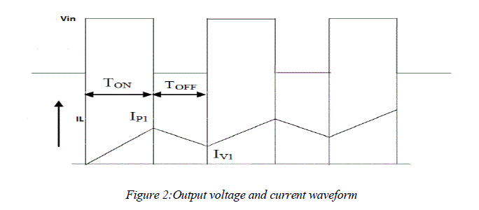 |
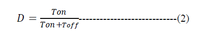
| When the MOSFET is turned ON, the voltage Vin is applied in reverse across the power diode. Therefore diode must stay OFF as long as MOSFET remains ON. The ON state of MOSFET always implies the OFF state of diode. With the MOSFET turned ON, current ILbeings to build up. The growth of IL occurs exponentially due to the inductance L. The MOSFET is kept ON for a time interval TON, and OFF for the interval TOFF. At the instant when MOSFET is turned OFF, IL has a finite value (IP1), which is the peak value of the output current during the first chopper cycle. This peak current occurs at the instant the MOSFET turns OFF. The presence of the inductance L prevents the sudden drop of IL to zero. The decay of IL causes an induced voltage L dil/dt to appear across the inductance. Because of this voltage, the diode becomes forward-biased and causes the current flow to continue and decay exponentially. The term “Free-Wheeling” is commonly used to describe the flow of current in this manner without the aid of a voltage source, but solely due to the stored energy in the inductance. The purpose of the diode is to provide the free-wheeling path for the MOSFET when it is turned OFF. Therefore, the diode automatically turns ON at the instant the MOSFET switches off due to the presence of an inductance with stored energy. The decay of IL continues as long as MOSFET remains OFF, that is, for a duration TOFF. The lowest value to which the current falls at the end of the first chopper cycle is labelled as the valley magnitude IV1 in Figure 2. The second chopper switching cycle commences when MOSFET is turned ON again at the end of the first TOFF, and the current again starts to build up. Due to the initial current IV1, the second peak IP2 will be larger than IP1. Consequently, the valley magnitude IV2 at the end of the second cycle will also be larger than IV1. In this way, as the switching progresses, both the peak and valley magnitudes progressively increase. After several cycles, the difference between successive cycles becomes negligibly small. We say that the circuit conditions have reached steady state [3,4]. This means that the peak current is effectively the same in successive cycles. A similar statement is true for the valley current. The relation between the input voltage (Vin), output voltage (Vout) and duty cycle (D) is given by: |
 |
Continuous and Discontinuous Current Modes |
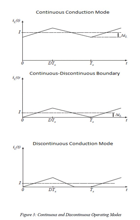
| If the value of the inductance is reduced to the critical point, the valley current will decay and finally become zero at the end of the duty cycle. A further decrease in L will cause the current to fall to zero even before the completion of the OFF period of the chopper. The current builds up from an initial zero value during TON in the next chopper cycle. This operation of the chopper is called discontinuous load current mode. If the current is nonzero for all the chopper period, the chopper is said to be operating in continuous load current mode. This is achieved by appropriate selection of chopper switching frequency or inductance value, or both. |
 |
IV.MODELLING IN SIMULINK |
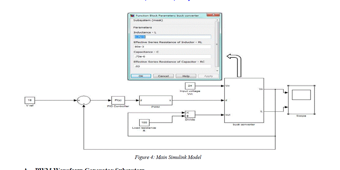
| The Simulink Model for the Buck Converter is shown in figure 4. The model consists of three constant blocks that are set by the user, namely: Input Voltage (Vin), Reference Output Voltage (Vref) and Load Resistance (Ro). |
| In addition to the Main Input parameters, the model consists of two more subsystems, namely:- |
| ïÃâ÷ PWM Generator: This subsystem accepts duty cycle in decimal form from the controller and outputs the required PWM waveforms of the corresponding duty cycle. |
| ïÃâ÷ Buck Converter: This subsystem includes all the blocks to model the Buck converter in mathematical form and produces the Output Voltage and Current waveforms based on its inputs. |
 |
A. PWM Waveform Generator Subsystem |
| This block is responsible for producing PWM pulses of varying duty cycle. As already explained, the circuit has two operating conditions, the Duty Interval (Ton) when the Chopper Switch is ON and the Free Wheeling mode (Toff) when the switch is OFF. To simulate both these conditions in the same model, switch blocks can be employed. However, the PWM pulses are easier to implement and also more convenient for our mathematical model, especially in the case of a closed loop system with a controller. The two inputs to the Subsystem are: |
| • The duty cycle from the controller in decimal form. |
| • Switching Frequency Fs, as a parameter in the mask as shown in figure 5. |
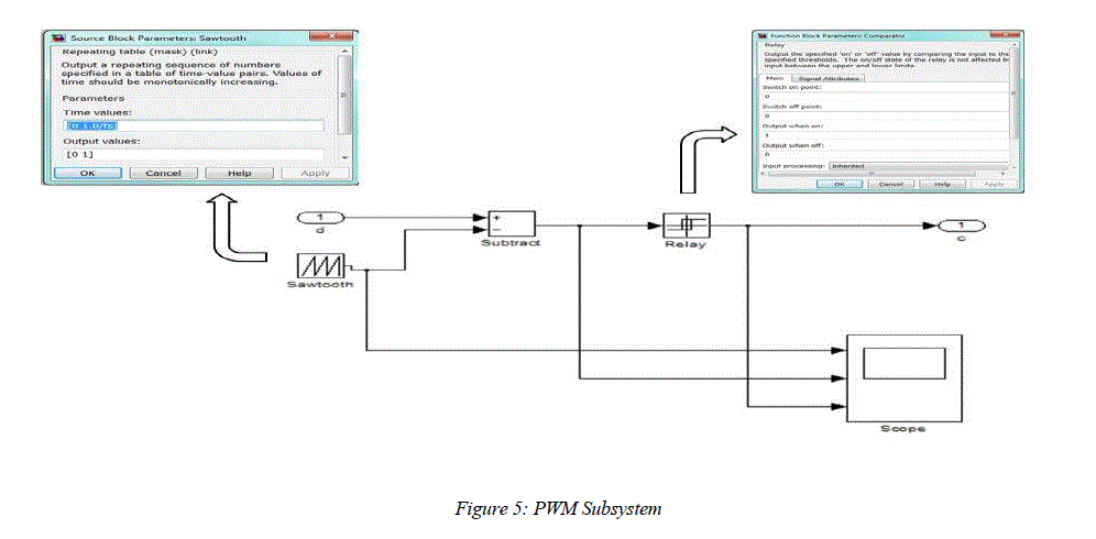 |
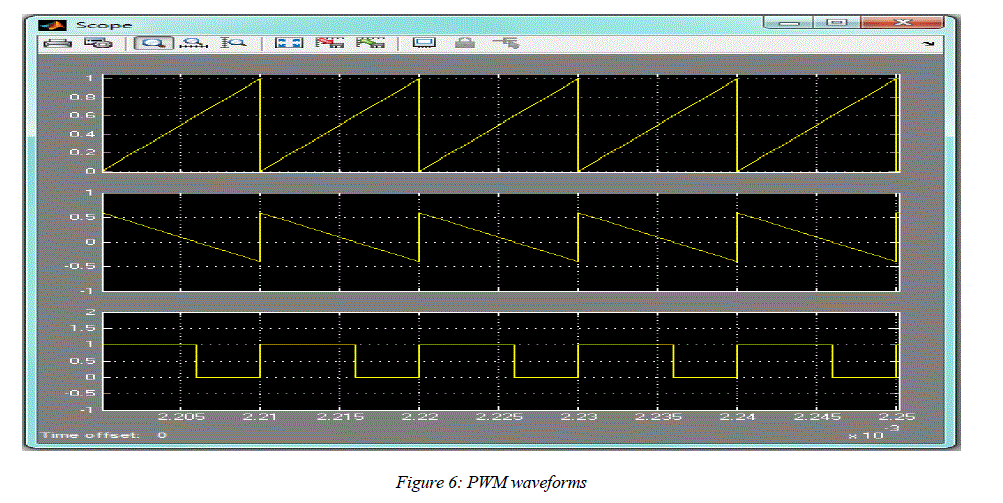
| Figure 6 shows the output waveforms of the subsystem for a constant 0.6 duty cycle. A Repeating Sequence Block (Waveform 1 in Figure 6) is inserted and configured to output a saw-tooth waveform of time values (0 1/fs) and Output Values (0 1). The magnitude of this waveform is subtracted from the duty cycle (decimal value) to yield a mirrored version of the saw tooth waveform whose amplitude ranges from D to D-1. This waveform (Waveform 2 in Figure 6) possesses a positive value whenever the required PWM signal is high and a negative value where the PWM pulse is low. This fact is exploited to generate the PWM pulses by using a Relay block that is configured to switch on (Output=1) and off (Output=0) during the zero crossings. The resulting waveform (Waveform 3 in Figure 6) is a PWM Signal of the required duty cycle. |
 |
B. Buck Converter Subsystem |
| This subsystem carries out almost all the computations to produce the Output Voltage and Load Current Waveforms. The inputs to the subsystem are the Input Voltage, Duty cycle and Load Current. In addition, the following values need to be declared as masked parameters: Inductance (L), Inductance Series Resistance (RL), Capacitance (C), and Capacitance Series Resistance (Rc). Underneath the mask is the actual implementation as shown in figure 7: |
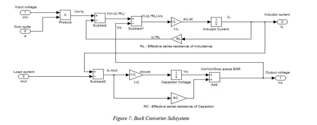 |
| The subsystem consists of two main loops, which are essentially differential equations which provide the Inductor Current and Output Voltage. |
| As stated in the principle of operations, the Buck Converter circuit has two modes of operation: |
| 1. The Duty Interval during which the chopper switch is closed and the input voltage source is applied across the Load. |
| 2. The Free Wheeling Interval during which the switch is open and the input voltage source is cut off from the Load. |
| To implement this in model form, we multiply the Input Voltage Vin with the PWM waveform. The result is that the Input Voltage is included in the KVL Equation when the PWM waveform is high (Vin×1=Vin) and omitted when it is low (Vin×0=0). |
| The first loop is responsible for computing the Inductor current by solving the differential equation obtained from applying KVL to Figure 1. |
 |
C. PID Controller |
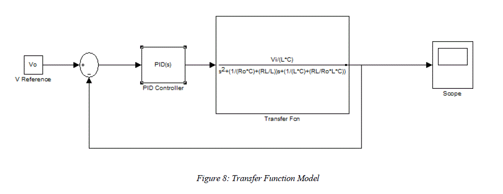
| The default PID controller Simulink block is utilized to generate the required duty cycle in decimal form (eg 45% duty cycle =0.45) based on the error signal. The P, I, and D parameters can be entered manually or can be tuned to some extent using the tools provided by Matlab, which also provides the Bode Plots for further analysis. However, an attempt to run the tuning tools will result in a linearization error as the forward path of the control loop linearizes to zero at certain points due to PWM logic. To circumvent this, the Buck Converter needs to be modelled as a Transfer Function to permit automatic tuning. |
 |
 |
| The tuned P, I and D parameters can then be substituted in the main model. Since the data can be exported to the workspace, one is free to implement their own control algorithms with the Fuzzy Logic, Neural Network toolboxes in Matlab or other computing techniques. |
V. VERIFICATION |
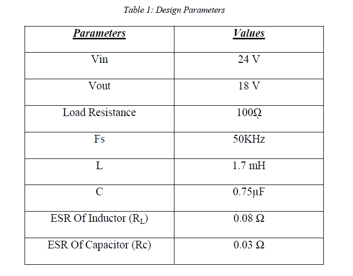
| A simulation run for a Buck Converter is carried out whose design parameters are specified in Table 1. |
 |
| The P, I and D values are obtained by using the Tuning tools provided by Matlab in the Transfer Function model as shown in Figure 8, and then substituted in the main model. |
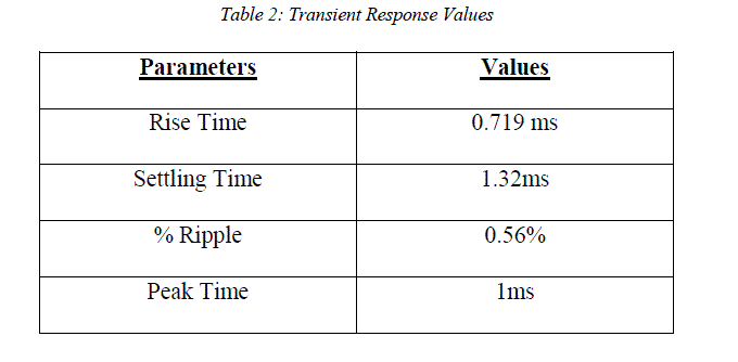 |
| To simulate a change in operating condition which is likely to happen in practical implementation, the Input voltage is stepped up to 25 V in the form of a pulse between time instants 0.003 to 0.006 to see if the controller maintains the required output voltage of 18V. The response is obtained as shown in Figure 9. |
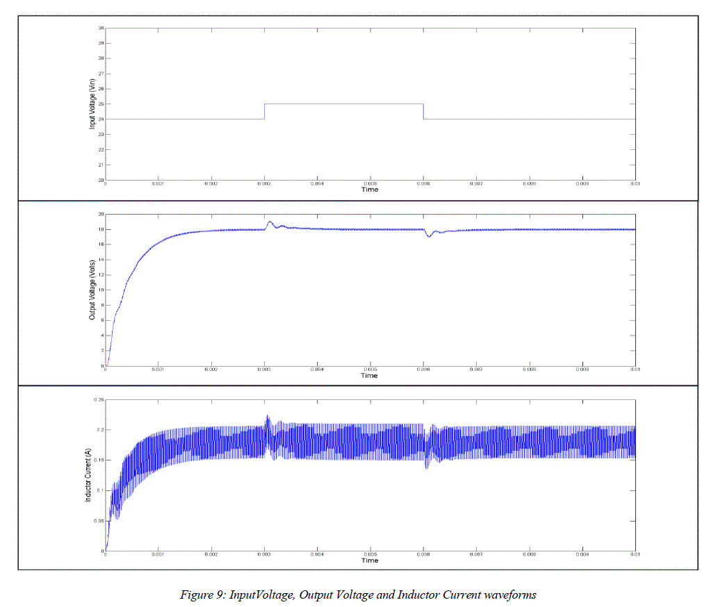 |
| The Output voltage rises to 18.8 V when the input voltage rises to 25 V and then reverts to 18V within 0.4 ms. Similarly, when the input voltage reverts to normal, a small ripple is experienced in the output voltage and current before it settles back to its steady state. The waveforms obtained from this model are nearly identical to a Buck Converter modelled using SimPowerSystems with only some minor deviation appearing in the Inductor Current. |
VI. CONCLUSION |
| In this paper, we have provided a brief overview of the operation of a Buck DC-DC converter, and proceeded to illustrate an alternate way to model the converter using only Simulink blocks, without the need of any SimPowerSystems. The mathematical model is derived from the system equations and provides an accurate representation of the Buck Converter. The Transfer Function of the system is also discussed in order to permit the use of the controller tuning tools provided by Matlab. One is free to replace the default PID block with their own algorithms. |
References |
|