International Journal of Innovative Research in Science, Engineering and Technology
ISSN ONLINE(2319-8753)PRINT(2347-6710)
ISSN ONLINE(2319-8753)PRINT(2347-6710)
| S. Anantha kumar Second year PG scholar, Bannari Amman Institute of Technology, Sathyamangalam, India |
| Related article at Pubmed, Scholar Google |
Visit for more related articles at International Journal of Innovative Research in Science, Engineering and Technology
In this paper modified single input multiple output dc-dc converters can be used to give a multi outputs. It has three outputs. That is low voltage power source is converted into high-voltage dc bus and middle voltage output terminals. It is coupled inductor based dc-dc converter. It has only one power switch with the properties of voltage clamping and soft switching. As a result, different level of output voltages, and multiple outputs, high efficiency power conversion and high step up ratio.
Keywords |
| MOSFET, VSI, PWM, ZCS, HVSC |
INTRODUCTION |
| This converter is a newly designed single input multiple output dc-dc converters with coupled inductor. The proposed converter uses only one power switch and main objective of high-efficiency power conversion, and different outputs, high step up ratio. The techniques of soft switching and voltage clamping are used to reduce the switching loss and conduction loss. a dc-dc converter is an electronic circuit which is used to convert a source of direct current (dc) from one voltage level to another voltage level. The boost Converter is a single input Single output device. To obtain multiple outputs, number of switches will be increases. This in turn increases the switching loss and stress. And that efficiency is low. The existing system is single-input single-output dc-dc converter with different voltage gains are combined to satisfy the requirement of different voltage levels, so this system control is complicated and cost is high. The existing system of the single input multi output dc-dc converter has a more then three switches for one output were required. In this method only suitable for low voltage and low power applications. The existing system of the dc –dc converter is generating buck, boost and inverter output simultaneously. However, over three switches for one output required. It is suitable for low voltage and low power applications. |
| High efficiency isolated boost dc-dc converter for high power low voltage fuel cell applications proposed by Morten Nyman and Michael A.E. Anderson deals with the high efficiency boost converter used for boosting the input voltage to obtain maximum output voltage here isolation provided using transformer. The proposed systems are increasing the conversion efficiency and reduce the manufacturing cost, voltage gain, and control complexity. The middle capacitor voltage is depends on auxiliary inductor. The output of the high-voltage dc bus can be controlled by a PI control. |
SINGLE INPUT MULTI OUTPUT DC-DC CONVERTER |
 |
| Fig. 1 Block diagram of single input multi output dc-dc Converter. |
| Fig. 1 shows the block diagram of single input multi output dc-dc converter. In this, the dc voltage from the source is fed into dc-dc converter, it could boost the input voltage and the boosted voltage is connected to various loads. This converter has a multiple output voltages. That is low voltage and middle voltage and high voltage output terminals. This converter is controlled by a PWM controller. |
| A. Circuit diagram of single input multi output dc-dc converter |
 |
| Fig. 2 Diagram for Single input multi output DC-DC Converter |
| Fig.2 shows the circuit diagram for single input multi output dc-dc converter. This converter can boost the voltage of a low voltage input power source to controllable high voltage dc bus and middle voltage output terminals. This converter has an only one power switch. The proposed converter is a coupled inductor based dc-dc converter. The output of the middle voltage output terminals can be appropriately adjusted by the design of auxiliary inductors |
| B. operating modes of dc-dc converter |
| MODE1: |
|
| Fig.3 Circuit diagram of Mode 1 operation |
| Fig.3 shows the Circuit diagram of Mode 1 operation. In this mode of operation the main switch s1 is turned ON. And diode D4 is turned OFF. Because the polarity of the coupled inductor Tr terminal is positive, the diode D3 turns ON. The secondary current iLS of the coupled inductor charges to the middle voltage capacitor C2. When the auxiliary inductor discharge the energy completely, at the end of the mode diode D2 turns OFF. |
| MODE 2: |
 |
| Fig.4 Circuit diagram of Mode2 operation |
| Fig.4 shows the Circuit diagram of Mode 2 operation. In this mode of operation the main switch S1 is still in ON condition. The magnetizing current ILMP increases gradually in linear way. Due to primary inductor charged by input power source. Middle voltage capacitor C2 is charged by secondary voltage I LS through the diode D3. Both the voltages Vlmp and vFC is equal in mode 1 and mode 2. The ascendant slope of the leakage current of the coupled inductor (diLKP/dt) at both mode1 and mode2 is different due to the path of the auxiliary circuit. The auxiliary inductors release its charges completely, at the end of the mode1 the diode D2 turns OFF. |
| MODE 3: |
 |
| Fig. 5 Circuit diagram of Mode3 operation |
| Fig.5 shows the Circuit diagram of Mode 3 operation. In this mode of operation the main switch S1 is turned off. The leakage current released from secondary side of coupled inductor charges the capacitor through diode D3. When the voltage across the main switch S1 is greater than the voltage across the capacitor C1, primary side leakage current is transmitted to auxiliary inductor Laux, and the diode D2 conducts. Auxiliary inductor supplies the load through diode D2.At the end of this mode diode D3 becomes reverse biased due to complete discharge of secondary side leakage current. |
| MODE 4: |
 |
| Fig.6 Circuit diagram of Mode4 operation |
| Fig.6 shows the Circuit diagram of Mode 4 operation. In this mode of operation the main switch S1 is persistently turned OFF. When the leakage energy has released from the coupled inductor primary side. The secondary current (iLS) of the coupled inductor is induced in reverse from the magnetising inductor Lmp through ideal transformer, and diode D4 is conducting the energy to the HVSC. At the same time primary side leakage inductor is still released to auxiliary inductor, the diode D2 keeps turn ON. The diodeD2 is conducting the auxiliary inductor current to output load. |
| MODE 5: |
 |
| Fig.7 Circuit diagram of Mode5 operation |
| Fig.7 shows the Circuit diagram of Mode 5 operation. In this mode of operation the main switch is still turn OFF; the primary leakage current is equal to the auxiliary inductor current. At the time diode D1 is turns OFF. The input power source is connected in series with primary winding of the coupled inductor Tr, and auxiliary inductor Lax, and supply the output load through diode D2.At the same time, the input power source is connected in series with secondary winding of the coupled inductor Tr, and middle voltage capacitor (C2), and to release the energy into the HVSC through the diode D4. |
| MODE 6: |
 |
| Fig.8 Circuit diagram of Mode 6 operation |
| Fig.8 shows the Circuit diagram of Mode 6 operation. In this mode of operation the main switch S1 is triggered. The input power source, clamped capacitor C1, coupled inductor secondary winding and middle voltage capacitor are connected in series, and energy release into the HVSC through diode D4. Diode D1 is a low voltage shotty diode; it will be cut off without a reverse-recovery current. The main switch is S1 is turned ON, ZCS condition and soft-switching is helpful to reduce the switching loss. At the mode of end the secondary current decays to zero. After that, next switching cycle is started and repeats the operation in the mode1. |
| DESIGN CONSIDERATIONS |
| The minimum resistances connected at the auxiliary circuit and the HVSC as |
 |
SIMULATION & RESULTS |
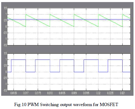
| The simulation of modified single input multi output dc-dc converter is done using MATLAB/SIMULINK software and the results are as follows.The simulation results are discussed and compared with the output voltage results. single input multi output dc-dc converter is simulated by using pulse width modulation technique.PWM technque is connected with input of the MOSFET gate terminal. |
PWM SWITCHING TECHNIQUE |
| Modified single input multi output dc-dc converter is simulated by using pulse width modulation technique. The reference signal and carrier waves are compared. The pulse is generated at reference wave is greater than the carrier wave. The pulse width modulation technique is connected with input of the MOSFET gate terminal. The pulse width is based on duty cycle. |
SOFT SWITCHING TECHNIQUES |
| There are two types of switching techniques, |
| ïÃâ÷ Zero voltage switching |
| ïÃâ÷ Zero current switching. |
ZERO VOLTAGE SWITCHING |
| Specifically means zero-voltage turn-on, the voltage across the device current increase is reduced to zero before the current increases |
ZERO CURRENT SWITCHING |
| Specifically means zero-current turn-off, the current flowing the through the device is reduced to zero before the voltage increases. |
| PWM switching technique |
 |
| Fig.9 Simulation model for PWM technique |
PWM SWITCHING FOR MOSFET |
 |
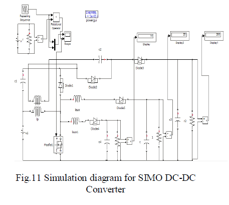
| SIMULATION CIRCUIT FOR MODIFIED SINGLE INPUT MULTIPLE OUTPUT DC-DC CONVERTER |
| Modified Single Input Multi Output DC-DC Converter can boost the voltage low voltage input source .That input voltage is 12V to controllable Boost the voltage is 14V,and High voltage is 200V, and middle output-voltage is 20-24V.The auxiliary inductor value is 2μH. And that capacitor value is c1=85μf, c2 value is 10μf.One coupled inductor is used. The primary of the coupled inductor is 2μH.secondary of the coupled inductor is 75μH. |
 |
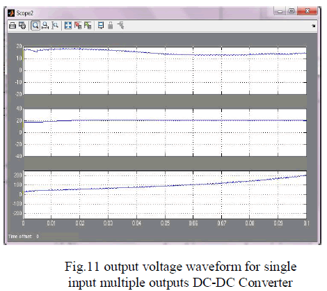
OUTPUT VOLTAGE WAVEFORM |
 |
CONCLUSION |
| This study has successfully developed a modified single input multiple output dc-dc converter with high efficiency. The simulation result shows the single input power source is converted to three output terminals. This topology adopts only one power switch to achieve the objective of multiple output with power conversion. |
References |
|