International Journal of Innovative Research in Science, Engineering and Technology
ISSN ONLINE(2319-8753)PRINT(2347-6710)
ISSN ONLINE(2319-8753)PRINT(2347-6710)
J. Joe Brislin1, J. Chelladurai2, B. Vinod3, M. Sundaram4
|
| Related article at Pubmed, Scholar Google |
Visit for more related articles at International Journal of Innovative Research in Science, Engineering and Technology
The main focus of the paper is to study the different modulation techniques used for three phase VSI supplying single phase loads that require neutral connection. Two types of topology of three phase inverter, namely three-leg and four-leg inverter are considered. PWM techniques used for both the topologies are described. The three dimensional space vector modulation used for four-leg inverter is discussed in a detailed manner. Though the four-leg inverters are less commonly used, it is the only possible solution for providing neutral connection to supply single phase loads from three phase inverter. The four-leg VSI presents advantages in a wide manner covering less dc link capacitance, high dc link voltage utilization and low distortion at output. The performance of various modulation strategies has been analyzed and verified using simulation in MATLAB environment.
Keywords |
| Fourleg inverter, 3DSVM, CBPWM |
INTRODUCTION |
| Power quality has become the most important issue in terms of industrial performance. Around 75 – 90 percent of industrial loads are non-linear loads. Non-linear loads have the inherent property of not allowing the steady state current to follow the applied voltage. Power losses in the low voltage distribution network due to the non-linear and non-symmetric loads account up to 10 percent of the average transmitted power. Thus, it is essential to limit these power quality deteriorating factors. Number of laws and standards involving power quality are imposed by providing limitations on current harmonics and voltage non-symmetry. When non-linear and non-symmetric loads are concerned, they pose serious problems in isolated systems like UPS, renewable energy sources operating in island mode and auxiliary power supplies. They also generate harmonics and cause unbalance along with flow of neutral current. |
| Numerous industrial solutions for current harmonics (active filters) and decreased power factor (capacitor banks) are already in practice successfully. At the same time, regarding recent times, there has been a huge increase in use of renewable energy sources as remote power generation units. Considering this development, non-symmetry with harmonic contamination has become an issue as they give simultaneous supply of three-phase and single-phase loads. |
| For high efficiency dc to ac conversion and peak power tracking, the inverter must have low harmonic distortion along with low electromagnetic interference and high power factor. There are several switching techniques to control voltage source inverter for harmonic reduction and for control for unbalanced loads. Pulse width modulation technique is the best one among them. They have become the de facto in the control of industrial standards. The performance of a modulation scheme can be evaluated based on output distortion, harmonic spectrum, dc link voltage utilization and complexity. In this paper the main focus will be simulation study of the modulation techniques applied on the three phase inverter supplying unbalanced loads. Various types of topologies of three phase inverter and their modulating techniques have been discussed. |
THREE LEG INVERTER |
| A three-phase inverter with three-leg consists of six power semiconductors arranged in three half-bridges, each including two power semiconductors. It generates a threephase power supply for a consumer from the voltage provided by the dc link. The desired magnitude and frequency of the output voltage can be obtained by controlling the switching action of devices in upper legs of inverter so that when averaged in time, a three-phase voltage is generated. This type of inverter is used largely for supplying balanced loads, powers ranging from few watts to more than megawatts. |
| Due to the absence of the neutral wire, this topology is unable to supply single phase loads.Since the source and load neutral are grounded at different potential, current flows in the soil due to load imbalance. This stray current of higher values can cause DC voltage oscillation and unbalance in the DC capacitor voltage. Therefore an isolated transformer is connected to the inverter output terminal. |
| The configuration shown in Fig. 1 is widely used and now it is possible to supply single phase loads.It has many advantages like galvanic isolation of primary and secondary voltage level, elimination of neutral current, overvoltage protection in certain cases and transformer inductance can be used in filter impedance. Transformer price and weight can be regarded as disadvantages in mobile applications like railways. |
| Two widely used PWM techniques for this topology are |
| 1) Sinusoidal pulse width modulation |
| 2) Space vector pulse width modulation |
 |
| Fig. 1 Three-leg voltage source inverter with isolated transformer topology |
| A. Sinusoidal Pulse Width Modulation |
| Sinusoidal pulse width modulation is widely used in power electronics to digitize the power so that a sequence of voltage pulses can be generated by the on and off of the power switches. Sinusoidal pulse width modulation switching technique is commonly used in industrial applications in motor control or solar vehicle applications. SPWM techniques are characterized by constant amplitude pulses with different duty cycle for each period. The width of these pulses are modulated to obtain inverter output voltage and to reduce its harmonic content. |
| In SPWM technique three sine waves and a high frequency triangular carrier wave are used to generate PWM signal. Generally three sinusoidal waves are used for three phase inverter. The sinusoidal waves are called reference signal and they have 120° phase difference with each other. The frequency of these sinusoidal waves is chosen based on the required inverter output frequency. The switching signal is generated by comparing the sinusoidal waves with the triangular wave. The comparator gives out a pulse when sine voltage is greater than the triangular voltage and this pulse is used to trigger the respective inverter switches. In order to avoid undefined switching states and undefined AC output line voltages, the switches of any leg cannot be switched off simultaneously. |
| The output of an inverter contain large amount of harmonics content since three phases are independently controlled and there is high voltage/current ripple due to the circulating energy. To the standalone load system where the loads are low voltage, the inverter is used without transformer but in case of utility grid or high voltage sensitive loads it should be used with step up transformer. As a result, due to the noise/ harmonic components the loss in the transformer will be increased by the presence of harmonics in the supply voltage and current. The complexity to implement the pulse width modulation is not complex as three analog comparators are enough. The maximum modulation index can range upto √3/2 |
| B. Space Vector Pulse Width Modulation |
| With a three phase voltage source inverter there are eight possible switching states which are represented as two nullvectors and six active-state vectors forming a hexagon. The voltage vector space is divided up into six sectors. The length of active state vectors are unity and the length of zero state vectors are zero. In one sampling interval, the output voltage vector can be obtained by having various turn on times of eight possible switching vectors. The decomposition of output voltage vector has infinite ways. However, in order to reduce the number of switching actions and make full use of active turn-on time for space vectors, the output vector is commonly split into the two nearest adjacent voltage vectors and zero vectors and in an arbitrary sector. |
 |
| Fig. 2 Vector representation for SVPWM |
| SVM now appropriates the rotating reference vector in each switching cycle by switching between the two nearest active-state vectors and the null-vectors.The vector for each switching state and the corresponding output voltages is shown in TABLE I. SaSbScdenote the switching states in A, B and C legs of the inverter respectively. |
 |
| TABLE I THREE LEG VSI OUTPUT VOLTAGES WITH RESPECTIVE SWITCHING STATES |
| In order to maintain the effective switching frequency of the power devices at a minimum, the sequence of toggling between these vectors is organized such that only one leg is affected in every step. The hexagon represents the range of realizable voltage space vectors. Using the space vector modulation process it is possible to realize any arbitrary voltage space vector that lies within this hexagon. The turn-on times for active vectors are identical in a different space PWM modulator. |
| The distribution of zero vectors yields different space-vector PWM modulators. There are no separate modulation signals in each of the three phases in spacevector modulation technique. Instead, a voltage vector is processed as a whole. For space-vector modulation, the boundary between the linear modulation range and the overmodulation range is the hexagon. The linear modulation range is located within the hexagon. If the output voltage vector exceeds the hexagon, it becomes greater than sampling time and is unrealizable. Thus, the overmodulation region for space-vector modulation is outside the hexagon. It is also noted that the trajectory of voltage vector should be circular while maintaining sinusoidal output line-to-line voltages.The vector has a length of 2/√3 Vdc, and a maximum modulation range of 2/√3 can be obtained. |
FOUR LEG INVERTER |
| For a three phase three wire systems, due to topology constraint, the sum of the three phase current is zero, thus there is no zero-sequence current. Only the positive sequence and negative sequence exist in the system. For a three phase inverter to supply single phase loads, neutral point must be provided. If the load is unbalanced, then the floating neutral on the load side makes an inherent unbalanced three phase output voltage because the zero sequence current cannot be controlled due to topology constraint. |
| It is already known that in a symmetrical system only two variables are independent, and as a result can be separately controlled (Xa+Xb+Xc = 0). On the other hand, nonsymmetrical systems have three independent variables (Xa+Xb+Xc ≠ 0). Separate control of three variables in threephase inverter is possible by providing a neutral connection for three phase four wire systems. The neutral connection can be provided by various topologies such as |
| 1) Split dc link capacitors where the neutral point is tied to the mid-point of the two dc link capacitors. |
| 2) Four-leg converter topology where the neutral point is tied to the mid-point of the fourth neutral leg containing two switches. |
| The first one, three phase inverter with split DC bus capacitors actually consists of three single-phase half bridge inverters and it suffers from an insufficient utilization of the dc link voltage. This enables the independent control of the each leg, i.e. phase. Single phase voltage supply is possible with this topology. With unbalanced loads neutral current returns through DC bus capacitors. The capacitor voltage is directly influenced by zero sequence current. For voltage balancing, large and expensive dc link capacitors are required to obtain an acceptable voltage ripple level across the dc link capacitors. |
 |
| Fig. 3 Four-leg voltage source inverter with split link dc capacitors |
| The three leg inverters with split dc link capacitors have a maximum modulation range of √3/2. This indicates that the DC link voltage utilization is 15% less than that would be achieved otherwise with a three legged power converter with space vector modulation. |
| On the other hand, the four-leg VSI with eight semiconductor switches can handle the neutral current without affecting the capacitor life. Many applications require the neutral connection. Renewable energy based generators and fuel-cell based generators which may run in either standalone or grid parallel mode, Active power filters which compensate the harmonic current through neutral point requires three phase output with neutral connection. Complex modulation schemes and large number of semiconductor devices can be sometimes considered a disadvantage. Nevertheless, this type of inverter is ideal solution in four-wire systems for supplying non-symmetrical and single-phase loads. |
 |
| Fig. 4 Four-leg voltage source inverter topology |
| The dc-link utilization factor will also improve by 15% compared to the three-leg VSI. With the additional leg, the switching states increase from 8 (23) to 16 (24) and thus, control flexibility and an improvement in the quality of the VSI output voltage can be achieved. Some common modulation techniques are, |
| 1) Carrier based PWM |
| 2) Three dimensional space vector PWM |
| A. Carrier based Pulse Width Modulation |
| This modulation technique is similar to sinusoidal PWM where switching states are determined by comparing triangular carrier and three sine reference waveforms. The only difference is in the reference waveform generation where additional offset voltage is added to sinusoidal waveform. Using this modification it is possible to have any type of switching sequence. Output line to neutral voltages Van, Vbn and Vcn can be rewritten by using respective leg voltages and common offset voltage Vn0. |
 (1) (1) |
| Maximum values of Van, Vbn and Vcnare ±Vdc. In three-phase three-leg inverter offset voltage is selected as |
 (2) (2) |
| With the help of fourth leg, Vn0 can be actively manipulated by the control of the gating signal of the additional leg. |
 |
| Fig. 5 Block diagram of Carrier based PWM technique |
| This simplified control scheme has limitations for the control of neutral leg and the dc link voltage utilisation is also limited to the voltage vector forming a polyhedron. |
| B. Three Dimensional Space Vector Pulse Width Modulation |
| The main purpose of using a SVPWM in a four leg inverter is to obtain the most inherent advantage of higher DC link voltage utilization. The SVPWM is based on the representation of the voltage reference in space vector on the αβγ plan. The αβγ components can be obtained through the Clarke’s transformation as shown in (3). Since the neutral connection is being considered, the zero-sequence component obtained from Clarke’s transformation is not zero. |
 (3) (3) |
| From the Fig. 4, it can be seen that the inverter topology has eight switches which yields sixteen (24) switching states in which two states have zero values. |
| The various voltage values with respect to Vdc for αβγ frameare shown in TABLE II. The vectors obtained from TABLE II can be used to built the three dimensional space for projecting the reference voltage vector. |
| The vectors denoted in TABLE II can be projected in three dimensional plane as shown in Fig. 6. The distribution of the sixteen switching vectors are shown in the three dimensional space. There are two zero switching vectors and fourteen non-zero switching vectors. It can be seen that each of the switching vector for a three legged converter splits into two switching vectors, depending on switching position of the neutral leg. The implementation of 3D-SVM can be done by the following steps |
| 1) Locating reference vector in three dimensional space. |
| 2) Calculating the duty cycle of the vectors for the corresponding switching time. |
| 3) Obtaining the switching sequence for a particular switching time. |
 |
| TABLE II FOUR LEG VSI OUTPUT VOLTAGES WITH RESPECTIVE SWITCHING STATES |
| The vector for each switching state and the corresponding output voltages is shown in TABLE II. SaSbScSd denote the switching states in A, B, C and D legs of the inverter respectively |
| 1) Synthesis of Reference Vector: A reference vector for three dimensional space vector modulation can be acquired using the switching vectors in αβγ plane. In order to obtain the reference vector, three non-zero space vectors should be used. To fulfil our primary aim of reducing the harmonic current and current deviation due to the switching during the modulation period, the selected vectors should be the adjacent ones to the reference vector. The selection of adjacent vectors also has some considerable effect on the switching losses. |
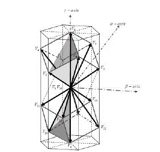 |
| Fig. 6 Representation of switching vector in αβγ plane |
| There are two major steps in identifying the reference vector. Similar to the six sectors in the two dimensional SVM, six prisms can be identified in three dimensional space. The projection of the reference vector in αβγ plane will determine the prism number. Each prism can be further broken down into four tetrahedrons accounting to a total of 24 tetrahedrons. The adjacent switching vectors are defined by the tetrahedron number. |
 (4) (4) |
 (5) (5) |
 (6) (6) |
| The variable Pfrom (4) to (7) can be used for prism identification on 3D SVM. Once the prism numberis obtained, the correct tetrahedron can be found by using (8) |
| The variable T returns a numerical value identifying the tetrahedron. From the TABLE III, the corresponding prisms and tetrahedrons according to the obtained variables P and T,will give the adjacent non-zero space vectors used for synthesizing the voltage reference V*. |
| 2) Duty Cycle Calculation: The duty cycle of the reference vector can be easily found from the adjacent vectors obtained from the tetrahedron number. |
| where Vr1, Vr2, Vr3 correspond to the non-zero space vectors and t1, t2 and t3 to the various voltage values with respect to Vdc. Since the space vectors Vr1, Vr2 and Vr3 and the reference vector V* are known directly from (9), it is possible to determine the time period t1, t2 and t3from (10). |
 (10) (10) |
| The modulation time ratio for the zero vectors can be obtained by (11). There are two zero vectors 1 and 16. The strategy to select the switching vectors will depend on the switching sequence defined for the gates activation. |
| 3) Sequencing the Switching Vectors: The time ratio for switching vectors was obtained and now it is necessary to define the sequence in which the vectors can be activated. The switching sequence does not affect the average value of the resulting voltage; it has influence only on the harmonic content of VSI output and also on the power losses. |
 |
| TABLE III ADJACENT VECTOR SELECTION |
| Many classes of switching sequence like symmetrically aligned and alternative sequence are there. Depending on the used strategy, one or both zero states may be used in the sequence. For each tetrahedron, there will be a different switching sequence, based on the class of switching sequence selected.Since each tetrahedron has different switching sequence, ti, tj, tk and tl will correspond to a different leg switching each time. For example, for Tetrahedron 1, by choosing ti = ta, tj = tn, tk = tb and tl= tc, the gates can be activated as symmetrically aligned case. Similarly the time instants for various switching sequences are obtained. |
 |
| TABLE IV TIME INSTANTS OF SYMMETRICALLY ALIGNED CASE |
| The time instant waveform obtained can then be compared with high switching frequency carrier waveform to obtain the switching signals. In this case the time instant waveform will act as the modulating signal. The order of the time instants to be reproduced for each instant is presented below in the TABLE IV. |
DISCUSSION AND SIMULATION RESULTS |
| A. Capacitor Selection |
| The capacitor selections for the four leg inverter involves the important terms of negative (In) and zero (Io) sequence current components. For four leg inverter with split link dc capacitor, two capacitors are connected parallel and the required capacitor value can be calculated as |
| The DC link will also have a ripple due to the load neutral current and the capacitor value must be able to handle the neutral current. |
| For four leg inverter, the capacitance value can be designed based on the negative sequence component and the voltage ripple caused by an unbalanced load. |
 (13) (13) |
| where, M refers to the modulation index. From the above selection design, it can be seen that in order to obtain the same voltage ripple, the four leg VSI has four times less value of capacitance than the value required for split link dc capacitor. |
| B. Simulation Results |
| The modulation techniques were simulated in MATLAB environment and the performance characteristics were analysed. Source and load parameters were retained for all the schemes, so that the performances can be evaluated for the same operating conditions. The parameters are tabulated in TABLE V. Filters are required on the AC side, as the output voltage is composed of discrete values. Therefore to compensate the attenuation frequency, filters are calculated and used. |
 |
| TABLE V PARAMETERS USED FOR SIMULATION |
| When unbalanced load conditions are considered, then there will be flow of neutral current depending on the amount of unbalance. For such unbalanced conditions, the zero sequence current will be present along with positive and negative sequence of currents. It can be seen from Fig. 7, that the capacitor voltage is directly influenced by zero sequence current. Hence for voltage balancing, high values of capacitors and additional balancing circuits have to be used. This increases the complexity to control the circuit and the total cost. |
 |
| Fig. 7 Voltage unbalance seen in four leg inverter with split link dc capacitor having unbalanced load |
| The first step of synthesising the reference vector includes the identification of prism and tetrahedron number as shown in the Fig. 8. When a balanced load is used, then the prism and tetrahedron number would be traced as shown above in a stepwise manner. If an unbalanced load is used, then the vector will trace the tetrahedron number according to its instantaneous values. The modulating signal to activate the switching gates is shown in Fig. 9 and it is used to calculate the on time for each switching vector by comparing it with a carrier wave. |
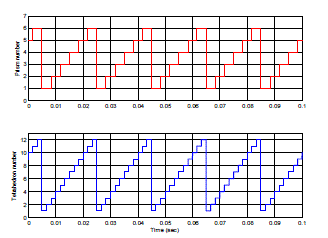 |
| Fig. 8 Prism and Tetrahedron number for balanced load and source in 3DSVM |
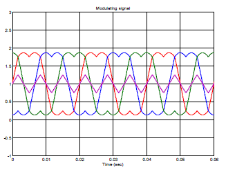 |
| Fig. 9 Modulating signal to activate switching states in 3DSVM |
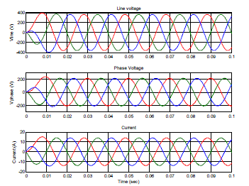 |
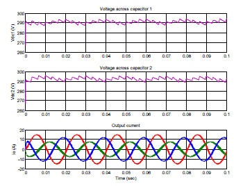
| Fig. 10 Three phase output voltage and current waveform of 3DSVM under balanced load condition |
| The 3DSVM system was analysed for various load conditions and THD was obtained. Fig. 10 and Fig. 11 shows the three phase output waveforms of voltage and current for various load conditions. For unbalanced load condition the tetrahedron will be found according to the voltage vector reference and it resides in tetrahedron values of 13 to 24 (i.e.) the lower half of the polyhedron. Requirement of DC link capacitor value is also minimum due to the use of four leg inverter and 3DSVM technique has an inherent property of having high DC link voltage utilization. As they contain only a single capacitor, handling it for circulating energy is not much complicated. THD analysis was performed for all the modulation strategies and the values are tabulated in TABLE VI. |
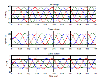 |
| Fig. 11 Three phase output voltage and current waveform of 3DSVM under unbalanced load condition |
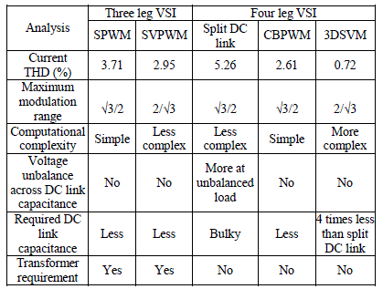 |
| TABLE VI PERFORMANCE EVALUATION FOR DIFFERENT MODULATION STRATEGIES |
CONCLUSION |
| The four-leg VSI is presented as a viable solution for handling with systems and loads that demands a neutral connectionand it can be seen from TABLE VI. Although the 3DSVM method may have a definition and a reference synthesis algorithm more complex than the three-leg case, it maintains the advantages of the traditional SVPWM implementation. Besides, it can also be seen that four-leg VSI demands a smaller DC link capacitanceof 1960μF when compared to split dc link capacitance that requires 6760 μF. The use of the 3-D SVPWM technique allows a higher utilization of the DC link voltage which make them an interesting alternative for high power applications and devices. Also, handling the DC link voltage in a single-capacitor configuration is simpler, and it avoids a high energy flow in the VSI DC link. |
References |
|