ISSN ONLINE(2319-8753)PRINT(2347-6710)
ISSN ONLINE(2319-8753)PRINT(2347-6710)
| V.Premchandran1, Sishir Sasi.P2, Dr.P.Poongodi3 Department of Electronics and communication Engg, PPG Institute of Technology, Coimbatore-35, India 1, 2, 3 |
| Related article at Pubmed, Scholar Google |
Visit for more related articles at International Journal of Innovative Research in Science, Engineering and Technology
A high-quality algorithm is proposed for VLSI implementation of an image scaling processor. The proposed image scaling algorithm consists of a sharpening spatial filter, a clamp filter, and a bilinear interpolation. To reduce the blurring and aliasing artifacts produced by the bilinear interpolation, the sharpening spatial and clamp filters are added as prefilters. To minimize the memory buffers and computing resources for the proposed image processor design, a T-model and inversed T-model convolution kernels are created for realizing the sharpening spatial and clamp filters. Furthermore, two T-model or inversed T-model filters are combined into a combined filter which requires only a one-line-buffer memory. Moreover, a reconfigurable calculation unit is invented for decreasing the hardware cost of the combined filter. Moreover, the computing resource and hardware cost of the bilinear interpolator can be efficiently reduced by an algebraic manipulation and hardware sharing techniques. The VLSI architecture in this work can achieve 280 MHz with 6.08-K gate counts, and its core area is 30 378 μm2 synthesized by a 0.13-μm CMOS process. Compared with previous lowcomplexity techniques, this work reduces gate counts by more than 34.4% and requires only a one-linebuffer memory.
INTRODUCTION |
| IMAGE scaling has been widely applied in the fields of digital imaging devices such as digital cameras, digital video recorders, digital photo frame, high-definition television, mobile phone, tablet PC, etc. An obvious application of image scaling is to scale down the highquality pictures or video frames to fit the minimize liquid crystal display panel of the mobile phone or tablet PC. As the graphic and video applications of mobile handset devices grow up, the demand and significance of image scaling are more and more outstanding. The image scaling algorithms can be separated into polynomialbased and non-polynomial-based methods. The simplest polynomial-based method is a nearest neighbor algorithm. |
| It has the benefit of low complexity, but the scaled images are full of blocking and aliasing artifacts. The most widely used scaling method is the bilinear interpolation algorithm by which the target pixel can be obtained by using the linear interpolation model in both of the horizontal and vertical directions. Another popular polynomial-based method is the bicubic interpolation algorithm [15], which uses an extended cubic model to acquire the target pixel by a 2-D regular grid. In recent years, many high-quality non-polynomial-based methods [2]–[4] have been proposed. These novel methods greatly improve image quality by some efficient techniques, such as curvature interpolation [2], bilateral filter [3], and autoregressive model [4]. The methods mentioned earlier efficiently enhance the image quality as well as reduce the artifacts of the blocking, aliasing, and blurring effects. However, these high-quality image scaling algorithms have the characteristics of high complexity and high memory requirement, which is not easy to be realized by VLSI technique. Thus, for realtime applications, low-complexity image processing algorithms are necessary for VLSI implementation [5]– [9]. To achieve the demand of real-time image scaling applications, some previous studies [10]–[15] have proposed low complexity methods for VLSI implementation. Kim et al.proposed the area-pixel model Winscale [10], and Lin et al.realized an efficient VLSI design [11] Chen et al. [12] also proposed an area-pixelbased scalar design advancd by an edge-oriented technique. Lin et al. [13], [14] presented a lowcost VLSI scalar design based on the bicubic scaling algorithm. In our previous work [15], an adaptive real-time, low-cost, and high-quality image scalar was proposed. It successfully improves the image quality by adding sharpening spatial and clamp filters as prefilters [5] with an adaptive technique based on the bilinear interpolation algorithm. Although the hardware cost and memory requirement had been efficiently reduced, the demand of memory still costs four line buffers. Hence, a low-cost and low-memory-requirement image scalar design is proposed in this brief. |
II. PROPOSED SCALING ALGORITHM |
| Fig. 1 shows the block diagram of the proposed scaling algorithm. It consists of a sharpening spatial filter, a clamp filter, and a bilinear interpolation. The sharpening spatial and clamp filters [6] serve as prefilters [5] to reduce blurring and aliasing artifacts produced by the bilinear interpolation. First, the input pixels of the original images are filtered by the sharpening spatial filter to enhance the edges and remove associated noise. Second, the filtered pixels are filtered again by the clamp filter to smooth unwanted discontinuous edges of the boundary regions. Finally, the pixels filtered by both of the sharpening spatial and clamp filters are passed to the bilinear interpolation for up-/ downscaling. To conserve computing resource and memory buffer, these two filters are simplified and combined into a combined filter. The details of each part will be described in the following sections. |
 |
A. Low-Complexity Sharpening Spatial and Clamp Filters |
| The sharpening spatial filter, a kind of high-pass filter, is used to reduce blurring artifacts and defined by a kernel to increase the intensity of a center pixel relative to its neighboring pixels. The clamp filter [6], a kind of lowpass filter, is a 2-D Gaussian spatial domain filter and composed of a convolution kernel array. It usually contains a single positive value at the center and is completely surrounded by ones [15]. The clamp filter is used to reduce aliasing artifacts and smooth the unwanted discontinuous edges of the boundary regions. The sharpening spatial and clamp filters can be represented by convolution kernels. A larger size of |
| convolution kernel will produce higher quality of images. However, a larger size of convolution filter will also demand more memory and hardware cost. For example, a 6 × 6 convolution filter demands at least a five-line-buffer memory and 36 arithmetic units, which is much more than the two-line-buffer memory and nine arithmetic units of a 3 × 3 convolution filter. In our previous work [15], each of the sharpening spatial and clamp filters was realized by a 2-D 3 × 3 convolution kernel as shown in Fig. 2(a). It demands at least a fourline- buffer memory for two 3 × 3 convolution filters. For example, if the image width is 1920 pixels, 4 × 1920 × 8 bits of data should be buffered in memory as input for processing. To reduce the complexity of the 3 × 3 convolution kernel, a cross-model formed is used to replace the 3 × 3 convolution kernel, as shown in Fig. 2(b). It successfully cuts down on four of nine parameters in the 3 × 3 convolution kernel. Furthermore, to decrease more complexity and memory requirement of the cross-model convolution kernel, T-model and inversed T-model convolution kernels are proposed for realizing the sharpening spatial and clamp filters. As shown in Fig. 2(c), the T-model convolution kernel is composed of the lower four parameters of the crossmodel, and the inversed T-model convolution kernel is composed of the upper four parameters. In the proposed scaling algorithm, both the T-model and inversed Tmodel filters are used to improve the quality of the images simultaneously. The T-model or inversed Tmodel filter is simplified from the 3 × 3 convolution filter of the previous work [15], which not only efficiently reduces the complexity of the convolution filter but also greatly decreases the memory requirement from two to one line buffer for each convolution filter. The T-model and the inversed T-model provide the lowcomplexity and low memory- requirement convolution kernels for the sharpening spatial and clamp filters to integrate the VLSI chip of the proposed low-cost image scaling processor. |
B. Combined Filter |
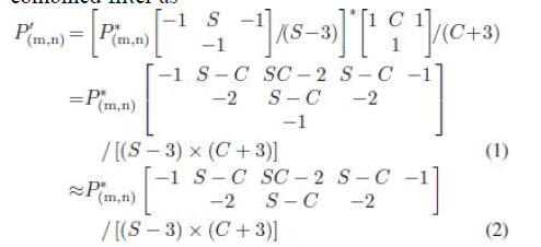
| In proposed scaling algorithm, the input image is filtered by a sharpening spatial filter and then filtered by a clamp spatial filter again. Although the sharpening spatial and clamp filters are simplified by T-models and inversed Tmodels, it still needs two line buffers to store input data or intermediate values for each T-model or inversed Tmodel filter. Thus, to be able to reduce more computing resource and memory requirement, sharpening spatial and clamp filters, which are formed by the T-model or inversed T-model, should be combined together into a combined filter as |
 |
| where S and C are the sharp and clamp parameters and P_ (m,n) is the filtered result of the target pixel P(m,n) by the combined filter. A T-model sharpening spatial filter and a T-model clamp filter have been replaced by a combined T-model filter as shown in (1). To reduce the one-line-buffer memory, the only parameter in the third line, parameter −1 of P(m,n−2), is removed, and the weight of parameter −1 is added into the parameter S-C of P(m,n−1) by S-C-1 as shown in (2). The combined inversed T-model filter can be produced in the same way. In the new architecture of the combined filter, the two T-model or inversed T-model filters are combined into one combined T-model or inversed T-model filter. By this filter-combination technique, the demand of memory can be efficiently decreased from two to one line buffer, which greatly reduces memory access requirements for software systems or hardware memory costs for VLSI implementation. |
C. Simplified Bilinear Interpolation |
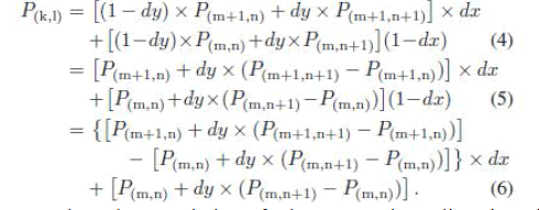
| In the proposed scaling algorithm, the bilinear interpolation method is selected because of its characteristics with low complexity and high quality. The bilinear interpolation is an operation that performs a linear interpolation first in one direction and, then again, in the other direction. The output pixel P(k,l) can be calculated by the operations of the linear interpolation in both x- and y-directions with the four nearest neighbor pixels. The target pixel P(k,l) can be calculated . |
| By (2), we can easily find that the computing resources of the bilinear interpolation cost eight multiply, four subtract, and three addition operations. It costs a considerable chip area to implement a bilinear interpolator with eight multipliers and seven adders. Thus, an algebraic manipulation skill has been used to reduce the computing resources of the bilinear interpolation. The original equation of bilinear interpolation is presented in (2), and the simplifying procedures of bilinear interpolation can be described from (4)–(6). Since the function of dy × (P(m,n+1) − P(m,n)) + P(m,n) appears twice in (6), one of the two calculations for this algebraic function can be reduced |
 |
| By the characteristic of the executing direction in bilinear interpolation [15], the values of dy for all pixels that are selected on the vertical axis of n row equal to n + 1 row, and only the values of dx must be changed with the position of x. The result of the function “[P(m,n) + dy × (P(m,n+1) − P(m,n))]” can be replaced by the previous result of “[P(m+1,n) + dy × (P(m+1,n+1) − P(m+1i,n))]” as shown in (6). The simplifying procedures successfully reduce the computing resource from eight multiply, four subtract, and three add operations to two multiply, two subtract, and two add operations. |
III. VLSI ARCHITECTURE |
| The proposed scaling algorithm consists of two combined prefilters and one simplified bilinear interpolator. For VLSI implementation, the bilinear interpolator can directly obtain two input pixels P_ (m,n) and P_ (m,n+1) from two combined prefilters without any additional line-buffer memory. Fig. 3 shows the block diagram of the VLSI architecture for the proposed design. It consists of four main blocks: a register bank, a combined filter, a bilinear interpolator, and a controller. The details of each part will be described in the following sections. |
A. Register Bank |
| In this brief, the combined filter is filtering to produce the target pixels of P_(m,n) and P_(m,n+1) by using ten source pixels. The register bank is designed with a oneline memory buffer, which is used to provide the ten values for the immediate usage of the combined filter. Fig. 4 shows the architecture of the register bank with a structure of ten shift registers. When the shifting control signal is produced from the controller, a new value of P(m+3,n) will be read into Reg41, and each value stored in other registers belonging to row n + 1 will be shifted right into the next register or line-buffer memory. The Reg40 reads a new value of P(m+2,n) from the linebuffer memory, and each value in other registers belonging to row n will be shifted right into the next register. |
B. Combined Filter |
| The combined T-model or inversed T-model convolution function of the sharpening spatial and clamp filters had been discussed in Section II, and the equation is represented in (1). Fig. 5 shows the six-stage pipelined architecture of the combined filter and bilinear interpolator, which shortens the delay path to improve the performance by pipeline technology. The stages 1 and 2 in Fig. 5 show the computational scheduling of a T-model combined and an inversed T-model filter. The T-model or inversed T-model filter consists of three reconfigurable calculation units (RCUs), one multiplier– adder (MA), three adders (+), three subtracters (−), and three shifters (S). The hardware architecture of the Tmodel combined filter can be directly mapped with the convolution equation shown in (1). The values of the ten source pixels can be obtained from the register bank mentioned earlier. |
| The symmetrical circuit, as shown in stages 1 and 2 of Fig. 5, is the inversed T-model combined filter designed for producing the filtered result of p_(m,n+1). Obviously, The T-model and the inversed T-model are used to obtain the values of p_ (m,n) and p(m,n + 1) _ simultaneously. The architecture of this symmetrical circuit is a similar symmetrical structure of the T-model combined filter, as shown in stages 1 and 2 of Fig. 5. Both of the combined filter and symmetrical circuit consist ofone MA and three RCUs. The MA can be implemented by a multiplier and an adder. The RCU is designed for producing the calculation functions of (S-C) and (S-C-1) times of the source pixel value, which must be implemented with C and S parameters. The C and S parameters can be set by users |
 |
| according to the characteristics of the images. The architecture of the proposed low-cost combined filter can filter the whole image with only a one-line-buffer memory, which successfully decreases the memory requirement from four to one line buffer of the combined filter in our previous work [15]. Table I lists the parameters and computing resource for the RCU. With the selected C and S values listed in Table I, the gain of the clamp or sharp convolution function is {8, 16, 32} or {4, 8, 16}, which can be eliminated by a shifter rather than a divider. Fig. 6 shows the architecture of the RCU. It consists of four shifters, three multiplexers (MUX), three adders, and one sign circuit. By this RCU design, the hardware cost of the combined filters can be efficiently reduced. |
C. Bilinear Interpolator and Controller |
| In the previous discussion, the bilinear interpolation is simplified as shown in (6). The stages 3, 4, 5, and 6 in Fig. 5 show the four-stage pipelined architecture, and two-stage pipelined multipliers are used to shorten the delay path of the bilinear interpolator. The input values of P_ (m,n) and P_ (m,n+1) are obtained from the combined filter and symmetrical circuit. By the hardware sharing technique, as shown in (6), the temperature result of the function “P_ (m,n) + dy × (P_(m,n+1) − P_ (m,n))” can be replaced by the previous result of “P_(m+1,n) + dy ×(P_(m+1,n+1)− P_(m+1i,n)).” It also means that one multiplier and two adders can be successfully reduced by adding only one register. The controller is implemented by a finite-state machine circuit. It produces control signals to control the timing and pipeline stages of the register bank, combined filter, and bilinear interpolator. |
IV. SIMULATION RESULTS AND CHIP IMPLEMENTATION |
| To be able to analyze the qualities of the scaled images by various scaling algorithms, a peak signal-to-noise ratio (PSNR) is used to quantify a noisy approximation of the refined and the original images. Since the maximum value of each pixel is 255, the PSNR expressed in dB can be calculated where M and N are the width and height of the original image. Furthermore, eight widely used test images [15] with the size 512 × 512 were selected for testing. In the quality evaluation procedure, each test image should be filtered by a fixed low pass filter (averaging filter) and then scaled up/down to different sizes such as 256 × 256 (half size), 352 × 288 common intermediate format (CIF), 640 × 480 video graphics array (VGA), 720×480 (D1), 1024×1024 (double size), and 1980× 1080 high-definition multimedia interface (HDMI) as listed in Table II. To show the quality of the images changed after using the clamp filter, sharp filter, and the proposed combined filter, the three kinds of PSNR results in this work are listed as A (sharp filter), B (clamp filter), and C (combined filter) in Table II. The experimental results show that this work achieves better quantitative quality than the previous low-complexity scaling algorithms [1], [10], [12]. The average PSNR of the bilinear interpolation [1] or this work is 28.15 or 28.54, which means that the combined T-model and inversed T-model filters improve the image quality by 0.39 dB. The quantitative qualities of bicubic (BC) [13] and our previous work [15] are better than this work because [13] and [15] obtain the target pixel by more complex calculation and refer to more neighboring pixels than this work. As listed in Table III, the multiplication operations of [13] are 32 which is eight times the quantity of this work, and the memory requirement of [13] or [15] is six or four lines which is six or four times the amount of the one-line buffer memory in this work. The VLSI architecture of this work was implemented by using the hardware description language Verilog. The electronic design automation tool Design Vision has been used to synthesize the VLSI circuit based on Taiwan Semiconductor Manufacturing Company 0.18- μm and 0.13-μm process standard cells. The layout for the proposed design was generated with IC Compiler. The chip photomicrograph is illustrated in Fig. 7. Furthermore, the proposed design was evaluated and verified by an field programmable gate array (FPGA) emulation board with an Altera FPGA EP2C70F896C6 core. As shown in Table IV, this work contains only 6.08-K gate counts, and the chip area is 30 378 μm2 synthesized by a 0.13-μm CMOS process. Moreover, this work can process the whole image with only a one-linebuffer memory. The power consumption of the proposed design was measured by using SYNOPSYS PrimePower. It consumes 6.9 mW at a 280-MHz operation frequency with a 1.1-V supply voltage. Furthermore, the throughput of this work achieves 280 megapixels per second. It is fast enough to achieve the demand of real-time graphic and video applications with a HDMI of WQSXGA (3200 × 2048) resolution at 30 frames per second. |
| Table IV lists the comparison results of six lowcomplexity VLSI designs with this work. As compared with the six previous designs, this work reduces at least 79%, 65%, 76.8%, 80.1%, 41.5%, or 34.5% gate counts than the previous designs of Win [10], Win [11], BC [13], BC [14], Edge-Oriented [12], or our previous work [15], respectively. Moreover, this work needs only a oneline- buffer memory, which is much less than four, six, or four of Win [10], [11], BC [13], [14], or our previous work [15], respectively. Consequently, this work provides a low-cost, low-memory-demand, high-quality, and high-performance VLSI design for real-time image scaling applications. |
V. CONCLUSION |
| In this brief, a low-cost, low-memory-requirement, high quality, and high-performance VLSI architecture of the image scaling processor had been proposed. The filter combining, hardware sharing, and reconfigurable techniques had been used to reduce hardware cost. Relative to previous low-complexity VLSI scalar designs, this work achieves at least 34.5% reduction in gate counts and requires only one-line memory buffer. |
References |
|