International Journal of Innovative Research in Science, Engineering and Technology
ISSN ONLINE(2319-8753)PRINT(2347-6710)
ISSN ONLINE(2319-8753)PRINT(2347-6710)
Kunal Subhash Khandelwal, Dr.A.K.Kureshi
|
| Related article at Pubmed, Scholar Google |
Visit for more related articles at International Journal of Innovative Research in Science, Engineering and Technology
LNA design meets different challenges because of its simultaneous requirements like good transistor selection, suitable DC biasing network, high gain, low noise figure, good input-output matching circuits, high linearity and good stability. In this paper we have chosen Avago Technologies ATF-58143. The results for Q-point, DC-Bias, Stability analysis are given using Agilent ADS.
Keywords |
| LNA, UWB, GaAs pHMET, Stability Condition, Impedance Matching, ADS |
INTRODUCTION |
| Demand of wireless communication systems with robust transmitting and receiving performance is growing tremendously due to the modern technology intense society. In wireless communications, receivers need to be able to detect and amplify incoming low power signals without adding much noise. Therefore a low noise amplifier (LNA) is often used as the first stage of these receivers. To design an LNA with trade-off or suitable compromise between gain and noise is always a matter of challenge |
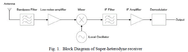
| A. Super-heterodyne Receiver |
| The basic function of LNA is to amplify the very weak received signal at the same time to minimize the noise power which is added to the received signals. By putting a BPF in before LNA reduces the possibilities to add other interfering signals to the desired signal, this is how, the amplifier cannot be overloaded with other high power signals. The output from LNA is feed to a mixer which is used to down convert the received radio signal to a lower frequency signal. A local oscillator (LO) is set at the level of the frequency which is near to the RF input and the output of the mixer will be relatively low and it could be filtered out by the IF band-pass filter. The high gain IF amplifier raises the power level of the filtered signal thus the baseband information can be recovered without distortion. |
 |
II. LNA DESIGN PARAMETERS |
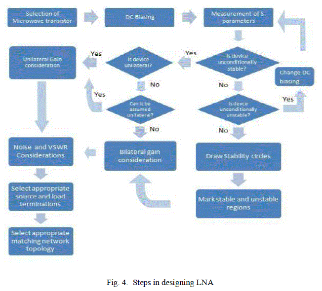
| The design procedure of LNA is described step by step in the following section. |
| A. Performance Trade-Offs in LNA |
| Different application has different requirement for LNA performance. The three important trade-offs are gain vs. power efficiency, linearity vs. drain-source dc current and LNA's gain vs. receiver's dynamic range. |
| B. Transistor Selection |
| Two commonly used categories of microwave transistors are: |
| (1) Silicon Bipolar Transistor (BJT) |
| (2) Gallium Arsenide Field Effect Transistors (GaAs FET) |
| a. Metal Semiconductor Field Effect Transistor (MESFET) |
| b. High Electron Mobility Transistor (HEMT) |
| 1. For application below 4GHz, BJTs have several advantages: |
| ïÃâ÷ Well established technology and hence lower cost & proven reliability. |
| ïÃâ÷ Low noise BJTs generally operate with lower bias currents and lower figures. |
| ïÃâ÷ BJTs are easier to match over a wide bandwidth and are normally unconditionally stable below 4GHz. |
| ïÃâ÷ The optimum source impedance for low-noise operation of BJTs leads to a smaller trade-off between noise performance and gain. |
| 2. Advantages of GaAs FET over BJTs |
| ïÃâ÷ Can operate at even higher frequencies, higher than 10GHz. |
| ïÃâ÷ Higher gain & lower noise figure (HEMTs have the best noise performance). |
| C. DC Biasing |
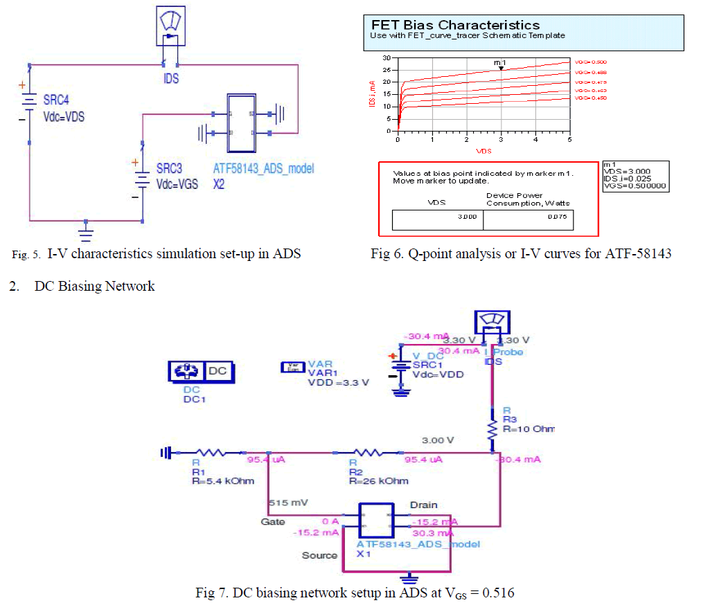
| Transistor must be biased at appropriate operating point before used. So that, transistor can works under values required and achieve less power consumption. If HEMT are to be used in design then proper selection of VDS and IDS should be taken by referring datasheet of transistor |
| D. Amplifier Power Gain Equations |
| An amplifier circuit can be modeled as a two-port network as shown below. Γs is the source reflection coefficient and ΓâÃâÃâ is the load reflection coefficient. |
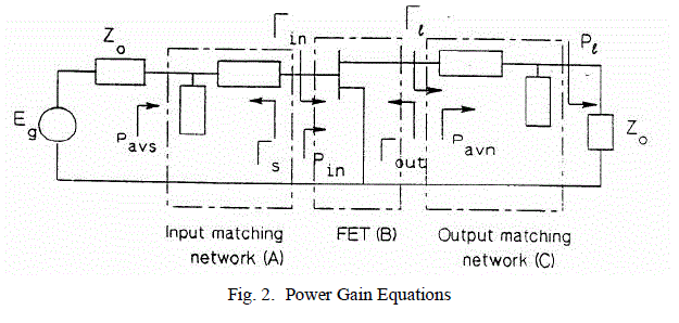 |
| From fig 2 the power definitions are expressed in as follows: |
| PAVS - Power available from source |
| PAVN - Power available from network, PIN - Power delivered to the input, PL - Power delivered to the load |
| Operating Power Gain = GP = PL/PIN, Available gain = GA = PAVN / PAVS, Transducer power gain = GT = PL / PAVS Power Gain Equations: The equations for the various power gain definitions are |
 |
| E. Noise in Amplifiers For low noise amplifier, the noise characteristic is what needs the designer pays special attention to during the design procedure. In a communication system, the LNA’s noise characteristic determines the system’s signal to noise (SNR) ratio and will be the bottle-neck of the data rata transmission. For multistage LNA, the NF is calculated with the following formulas |
| NF=NF1 + (NF2 -1) / G1 + (NF3-1) / G1G2 |
| NF is the noise figure of the system. |
| NFn is the noise figure of the NO.n stage. |
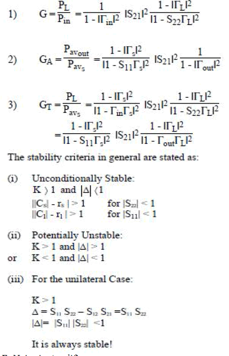
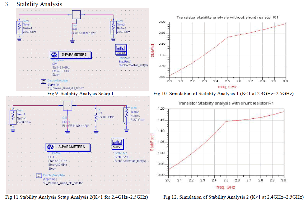
| From (1), we can see that the noise performance of the first stage determines the noise characteristics of the LNA, and the effect of the second stage is reduced by the gain of the first stage. Thus, the first stage should be ensured to have a low noise figure and high gain to obtain good noise performance of the LNA. F. Amplifier stability Design Oscillation is possible if the LNA is not stable, that will result in the failure of the design. There are two type of stability: unconditional stability and conditional stability. The conditional stability means that it can only keep stable in a certain range of passive source and load impedances; it is potentially unstable. To the contrary, the unconditional stability ensures the network to be stable for all passive source and load impedances. If it is possible, the designer should have a unconditional stability. In general, we judge whether the LNA is unconditionally stable by K-Δ test. It can be shown that the LNA will be unconditionally stable if the following necessary and sufficient conditions are met: |
| K = (1-| S11 |2 - | S22 |2 +| Δ|2 ) / 2 | S12S21 |>1 |
| | Δ| = | S11S22 - S12S21|<1 |
| (3) But the K-âÃâó test can’t be used to compare the relative stability of two or more devices. In 1992, Marion Lee Edwards had derived a new criterion to determine unconditional stability. μ=(1-| S11 | ) / (|S22 -ïÃâ¬Ã ΔS11* | + | S12S11|) >1 |
| (4) If μ>1, the LNA is unconditional stability, and the larger value of μ, the greater stability of the LNA. There are many approaches to improve the stability of the LNA such as source negative feedback, using attenuation network. In our design we use source negative feedback to ensure the LNA to be unconditional stability. |
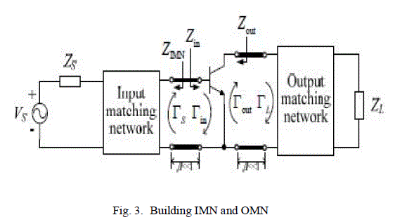
| G. IMN and OMN |
| Input and output of LNA must possess a stable input and output impedance for about 50 Ω over the frequency range of interest. To realize maximum gain, the input and output matching networks are simultaneously conjugate matched to the transistor. Maximum power transfer from the input matching network (IMN) to the transistor occurs when the two are conjugate matched so that ZIN = ZIMN. For the real valued system impedance, this leads to the requirement |
| (5) Maximum power is transferred from the transistor to the output matching network (OMN) when |
 |
 |
| H. Amplifier Topologies |
| ïÃâ÷ Reflective Match Amplifier |
| ïÃâ÷ Feedback Amplifier |
| ïÃâ÷ Balanced Amplifier |
| ïÃâ÷ Distributed Amplifier |
III. SELECTION OF MICROWAVE CAD TOOL |
| Computational optimization allows a complete sensitivity analysis to be carried out and leads to more accurate designs and a final tuned design in the first build; known as ‘first pass design success’. As it takes far less time to complete a final design, it is more cost effective than the traditional methods |
| Short summary of Microwave Design software is as follows: |
| ïÃâ÷ AWR Microwave Office |
| ïÃâ÷ Agilent Genesys |
| ïÃâ÷ Ansoft Designer RF |
| ïÃâ÷ Agilent ADS |
| ïÃâ÷ HSPICE/SONNET/LINC2 |
| ïÃâ÷ Cadence Spectre RF |
| ïÃâ÷ WIPL-D |
| ïÃâ÷ Pedasoft EM Supreme |
| ïÃâ÷ IE3D SSD (Mentor Graphics) |
IV. RESULT |
| Agilent ADS tool is used to obtain results. |
| 1. Q-Point Determination |
| Q point is chosen according to data sheet in which it is possible to get the minimum noise figure at 2.45 GHz which is the central frequency. |
 |
 |
V. CONCLUSION |
| In this paper we have discussed that LNA design is critical task. As there are many steps it is mandatory that proper care is taken at each step. These papers discuss Q-point analysis, Dc-Bias Analysis, Stability Analysis using s2p file from Avago Technologies website. At fig 2.45 GHz the stability factor with shunt resistance and without shunt resistor. The simulation is carried out using ADS Tool |
References |
|