International Journal of Innovative Research in Science, Engineering and Technology
ISSN ONLINE(2319-8753)PRINT(2347-6710)
ISSN ONLINE(2319-8753)PRINT(2347-6710)
Kiruba.T , Santhi.M
|
| Related article at Pubmed, Scholar Google |
Visit for more related articles at International Journal of Innovative Research in Science, Engineering and Technology
In this paper, an interleaved boost converter with zero-voltage transition and zero-current transition characteristics is proposed. The interleaved approach reduces the ripple of the input current and output voltage. The active snubber cell provides main switch to turn ON with zero-voltage transition (ZVT) and to turn OFF with zero-current transition (ZCT). All semiconductor devices operate with soft switching. There is no additional voltage stress across the main and auxiliary components. The proposed converter has simple structure, minimum number of components, and ease of control. The operating principle and detailed steady-state analysis of the converter are given. The proposed converter is simulated using MATLAB/SIMULINK
Keywords |
| soft switching, zero-voltage transition (ZVT), zero-current transition (ZCT), interleaved boost converter. |
INTRODUCTION |
| An Interleaved boost converter usually combines more than two conventional topologies and the current in the element of the interleaved boost converter is half of the conventional topology in the same power condition. Besides, the input current ripple and output voltage ripple of the interleaved boost converter are lower than those of the conventional topologies. The single boost converter can use the zero-voltage transition (ZVT) and/or zero-current transition (ZCT) to reduce the switching loss at the high frequency switching [1]-[9]. High-Frequency PWM dc–dc converters have been widely used in power factor correction, battery charging, and renewable energy applications due to their high power density, fast response, and control simplicity. To achieve high-power density and smaller converter size, it is required to operate converters at high switching frequencies. However, they are considered for the single topology. Many soft-switching techniques are introduced to the interleaved boost converter. In [10] the Zero-current-switching performance is used to reduce the switching losses by using coupled inductors in the interleaved boost converter.The cost of the converter is increased due to the usage of the coupled inductors. |
| In [11], [12], [13] zero voltage switching (ZVS) and zero current switching (ZCS) characteristics is achieved for the main switches of the interleaved boost converter. The ZVS and ZCS can operate only at variable frequency control to regulate the output. This is undesirable since it complicates the control circuit and generates unwanted EMI harmonics especially under wide load variations. In some papers [14] only ZVT characteristics is alone achieved for the main switches of the interleaved boost converter. This paper proposes an interleaved boost converter with an active Snubber cell is proposed. The active snubber cell provides both characteristics of zero-voltage transition during turn ON of the switch and zero-current transition during turn OFF of the switch. The proposed converter is the parallel of two boost converters with their driving signals stagger 180 and this makes the operation assumed symmetrical. The converter has simple structure, minimum number of components, and ease of control. |
II. OPERATION MODES AND ANALYSIS |
| A. Definitions and Assumptions |
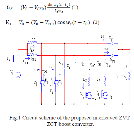
| Interleaved ZVT-ZCT PWM boost converter circuit is shown in Fig.1. In this circuit, input voltage source isVi, output voltage isVo,LF,LF1, is main inductor, CFis output filter capacitor, and DF,DF1 is main diode. The main switch S1, S3 consist of a main transistor T1, T3 and its body diode D1, D3. The snubber circuit shown with dashed line is formed by snubber inductor LS, LS1 a snubber capacitor CS, CS1and auxiliary switch S2, S4 consist of a transistor T2, T4 and its body diode D2, D4. The capacitor Cr, Cr1is assumed to be the sum of the parasitic capacitor of T1, T3 and the other parasitic capacitors incorporating it. In the proposed converter, it is not required to use an additional Cr capacitor. |
| B. Operation Modes of the converter |
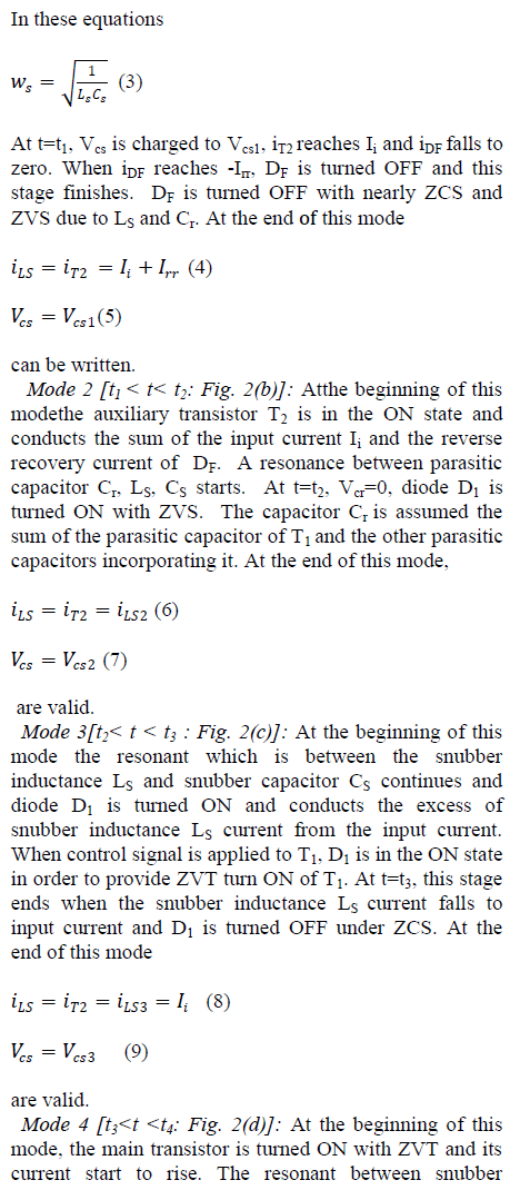
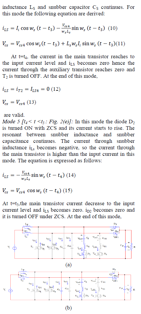
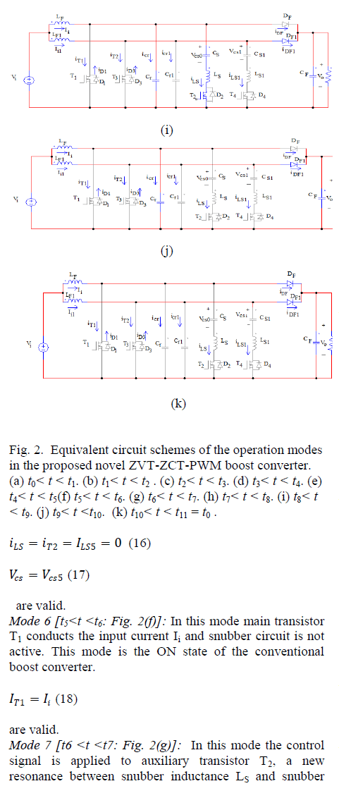
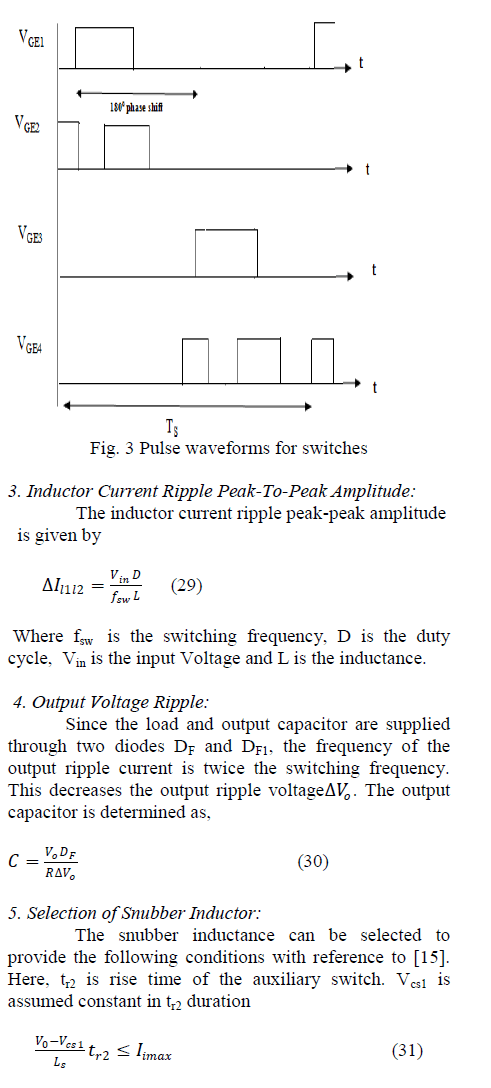
| In Fig. 2(a)-(k), the equivalent circuit diagram of the operation modes are given respectively. The pulse waveforms for switches are shown in Fig. 3. The detailed analysis of the proposed circuit is presented below. |
| Mode 1[t0 < t <t1: Fig.2 (a)]: At the beginning of this mode the main diode DF is in the ON state and the input current Ii flows through the main diode. The main transistor T1 and auxiliary transistor T2 are in OFF state. The initial voltage of the CS determines the soft-switching range of the circuit. At t=t0, a resonance starts between snubber inductance LS and snubber capacitor CS. Due to the resonance T2 current rises and DF current falls. The rise rate of current is limited by the snubber inductance LS connected serially to the auxiliary switch so that the turn ON of the auxiliary switch is provided with ZCS for this interval, the following equations can be written: |
 |
 |
 |
 |
 |
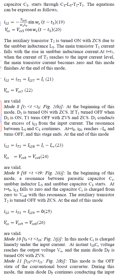 |
| current Ii and the snubber circuit is not active. For this mode ïÿýïÿýïÿýïÿýïÿýïÿý = ïÿýïÿýïÿýïÿý (27) can be written. Mode 12-22:since two cells of the converter are identical and operating with the same frequency and duty cycles and there is only 1800 phase shift between these two cells, the circuit behavior during operation modes of 11-22 is similar to that of during modes of 1–11. The circuit analysis of the converter during the last eleven modes is similar to that of the first eleven modes and can be Achieved by replacing T1, T2, D1, D2, DF, LF, Cr, LS, CS,Vcs0 with T3, T4, D3, D4, DF1, LF1, Cr1, LS1, CS1,Vcs1 respectively. |
III DESIGN PROCEDURE |
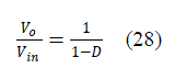
| The design procedure for the proposed interleaved ZVT-ZCT boost converter is presented in this section. 1. Operating Requirements: Output power Pout: 1KW Input voltage Vin: 200V DC Switching frequency (fsw): 100 KHZ Output voltage (Vo): 400V 2. Input and Output Parameters: The relationship between the duty cycle and the Output/input ratio for interleaved boost converter is |
 |
 |
 |
IV. SIMULATION RESULTS |
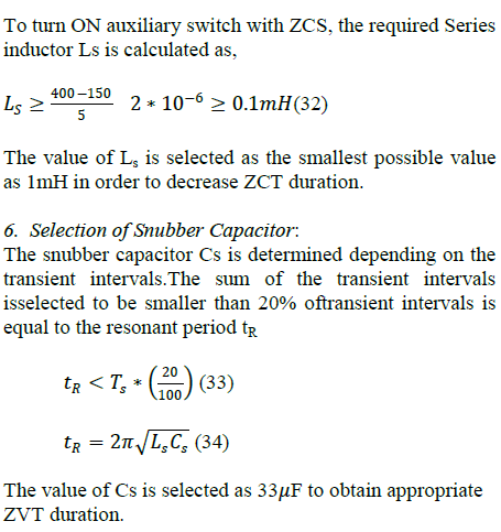
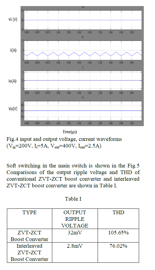
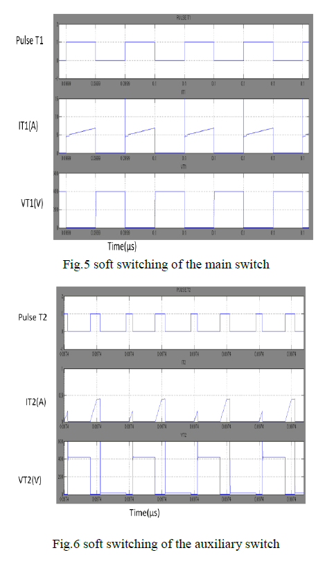
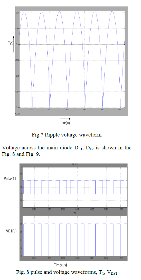
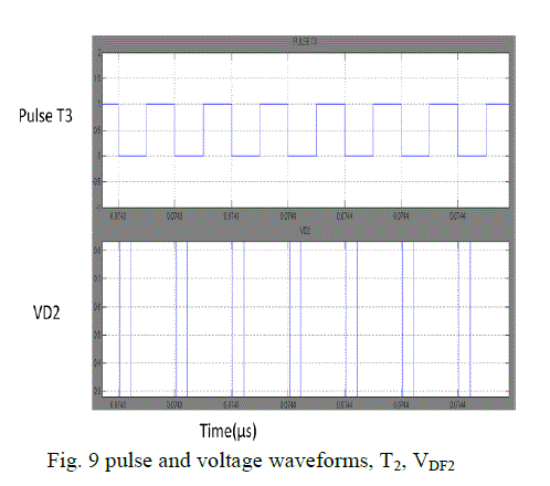
| The computer simulation of proposed converter is done using MATLAB/SIMULINK and the results are presented. The simulation result of the output voltage and output current are shown in Fig. 4.Soft switching in the auxiliary switch is shown in the Fig.6. Fig.7. Shows the Ripple content in the output voltage.Ripple content in the output voltage is low due to interleavingtechnique. Ripple content in the output voltage is calculated by finding the difference between peak –to–peak voltages. Due to reduce in the ripple content in the output voltage efficiency of the converter is increased. |
 |
 |
 |
 |
V. CONCLUSION |
| Interleaved ZVT-ZCT PWM boost converter is proposed in this paper. Hence, the input current ripple is reduced and the voltage stresses of the switches are greatly reduced compared with the conventional boost topology. This leads to the significant reduction of the conduction losses. Also, the switching losses is reduced by using an active snubber cell which provides ZVT turn on and ZCT turn OFF together for the main switch of the converter. Also, the proposed snubber cell is implemented by using only one quasi-resonant circuit without an important increase in cost and complexity. In the proposed converter, all semiconductor devices are switched under soft switching. The main diode is not subjected to any additional voltage and current stresses. The operation principles and steady-state analysis of the proposed converter are presented. The proposed converter is analyzed, design considerations are discussed, and its various operating modes are presented. The proposed converter was more efficient than the conventional boost converter. |
References |
|