International Journal of Innovative Research in Science, Engineering and Technology
ISSN ONLINE(2319-8753)PRINT(2347-6710)
ISSN ONLINE(2319-8753)PRINT(2347-6710)
V.Kumar1,2, M.Saroja1, M.Venkatachalam1, S.Shankar1
|
| Related article at Pubmed, Scholar Google |
Visit for more related articles at International Journal of Innovative Research in Science, Engineering and Technology
ZnS thin films were prepared using chemical bath deposition method and their optical and structural properties were studied. The ZnS thin films were grown on well cleaned glass substrates by hydro thermal method from aqueous solution of Zinc Sulphate and Thiourea at different growth temperatures. The properties of ZnS thin films and their growth mechanisms were studied using x-ray diffraction, SEM, EDAX, UV-Visible spectroscopy and photoluminescence measurements. Effect of growth temperature on structural and optical properties was reported
Keywords |
| ZnS, Hydro thermal, Growth temperature, Structural and Optical properties. |
I. INTRODUCTION |
| Semiconductor materials are always in the focus in material science due to their attractive electronic and optical properties and extensively potential applications in various fields. ZnS is a direct wide band gap semiconductor which has attracted much attention due to their vast potential in various fields. It has a high refractive index and a high transmittance in the visible range and is vital in the field of photonics. ZnS thin film has been proven as one of the promising thin film materials for detector, emitter, and modulators in optoelectronics It is potentially important material to be used as an antireflection coating for heterojunction solar cells [1], for light emitting diode [2] and other optoelectronic devices such as blue light emitting diode [3], electro luminescence devices and photovoltaic cells which enable wide application in the field of displays [4], sensors and lasers [5]. ZnS thin films have been produced using various techniques such as thermal evaporation [6], molecular beam epitaxy [7], chemical bath deposition [8], spray pyrolysis [9], RF reactive sputtering [10 ] and chemical vapor deposition [11]. Among them, chemical bath deposition is the commonly used method for production of ZnS layers. |
| CBD is a simple, convenient and inexpensive method. The process should be easily adaptable to large area processing with low fabrication cost. Thin films deposited by this method can be of high quality and studies of the deposition of ZnS by CBD form the subject of the present work. The properties of ZnS thin films vary depend on the various parameters such as growth method, temperature, precursor, pH, etc. In this work, ZnS thin films deposited on substrate using hydrothermal process by varying the growth temperature. The prepared samples were characterized by using Xray diffraction (XRD), SEM, EDAX, UV-Visible spectroscopy and Photoluminescence (PL) spectroscopy. |
II. EXPERIMENTAL DETAILS |
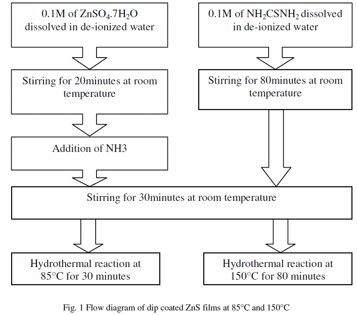
| ZnS films were prepared using dip coating method. The Zinc Sulphate solution was prepared by adding Zinc Sulphate (ZnSO4.7H2O) with the de-ionized water and this mixture was stirred with magnet for 20 minutes. Then Ammonia was added as a complexing agent on this ZnSO4 solution drop by drop and solution was stirred continuously around 80 minutes. Thiourea solution was prepared by adding it with the de-ionized water and this mixture was stirred with magnet for 60 minutes. |
| In the ZnSO4 prepared solution, Thiourea solution was added drop by drop and this mix was continuously stirred with the magnet for 30 minutes. A set of well cleaned substrates were dipped into that final solution at two different temperatures i.e. 85°C and 150°C. Fig (1) shows the flow diagram of dip coated ZnS thin films deposited at 85°C and 150°C. |
 |
III. CHARACTERIZATION TECHNIQUES |
| The structural characterization of the films was carried out using X-ray diffractometer with CuKα radiation (α=1.5404Å) in 2θ range from 10° to 80°. The SEM images and elemental compositions of the ZnS are analyzed by Scanning Electron Microscopy. The composition of the formed ZnS is determined by EDS analysis attached to a SEM instrument. The optical properties like absorption and transmission spectra were taken using a UV spectrophotometer in the range 100 to 1600 nm. Photoluminescence (PL) spectra were recorded using luminescence spectrometer. |
IV. RESULTS AND DISCUSSION |
| Fig (2) shows the XRD patterns of the obtained ZnS samples prepared at different growth temperatures of 85°C & 150°C. The patterns (black coloured) of ZnS samples prepared at 85°C show the peaks at 14.35° and 21.49° which correspond [12] to (005) and (006) diffraction planes. As seen, the (005) peak has the strongest intensity. All the diffraction peaks could be indexed to hexagonal structure of ZnS (JCPDS: 72-0163). |
| The XRD patterns (red coloured) of 150°C show the peaks at 31.87, 34.56 and 36.33° which correspond [13] to (104), (106) and (0010) diffraction planes. As seen, the (106) peak has the strongest intensity. All the diffraction peaks could be indexed to hexagonal structure of ZnS (JCPDS: 39-1363). |
| The XRD patterns clearly show the presence of ZnS, where all diffraction peaks is well indexed to the standard diffraction pattern of wurtzite-8H hexagonal ZnS phases. The average grain size of ZnS was estimated by using the well-known Scherrer’s formula [14], |
| D = 0.94λ / βcosθ |
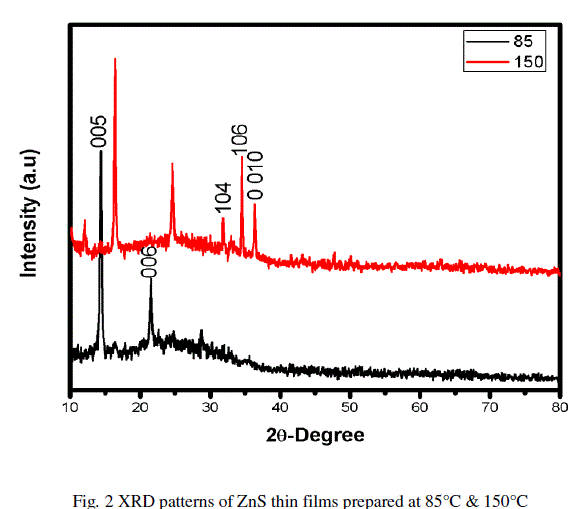 |
| Where λ = 1.5404Å for CuKα, β is the full width at half maximum (FWHM) of the peak corrected for the instrumental broadening in radians and θ is the Bragg’s angle. The average grain size of ZnS thin films at 85°C and 150°C were found to be about 38 nm and 74 nm respectively. |
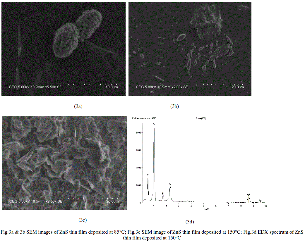
| The prepared ZnS samples were analyzed on a Scanning Electron Microscope (SEM). TheScanning Electron Microscopy (SEM) is a versatile technique for studying microstructure of thin films. The ZnS thin film prepared at 85°C and 150°C were used to study the surface morphology using a scanning electron microscope. Fig 3(a,b,c) show the SEM images of ZnS thin films prepared at 85°C and 150°C. The deposited material has an extremely high yield on the substrate and shows very easy reproducibility. The estimated average grain size of ZnS thin films prepared at 85°C and 150°C is 38 nm and 74 nm respectively. It is observed that the film is uniform whitish and well substrate covered. |
 |
 |
| In order to identify the constituent of these synthesized samples, typical EDS analysis was conducted for ZnS thin films prepared at 150°C to demonstrate that these samples are ZnS thin film. The composition analysis by EDS shown in fig (3d) demonstrates that the product contains only Zn and S, and no organic residues are detected. |
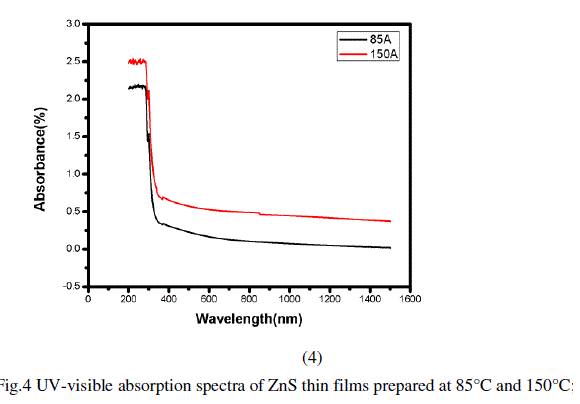
| To investigate the optical properties of the prepared ZnS thin films, UV-vis absorption spectra were recorded, as shown in fig (4). The optical absorption edge is approximately located at 286nm. An increase of the absorption values is observed with increase in deposition temperature. |
 |
| An estimation of the band gap value was obtained by the intersection point of the tangent of the absorption edge. The obtained band gap value is about 3.53eV for both ZnS thin films, which compares favourably with the literature value for hexagonal ZnS, measured at room temperature, of 3.54eV [15]. |
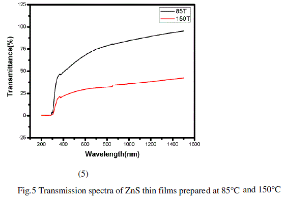
| Transmission spectra of both ZnS thin films at 85°C and 150°C were depicted in fig (5). A decrease in the transmission values over the whole spectral range is observed with increase in deposition temperature. |
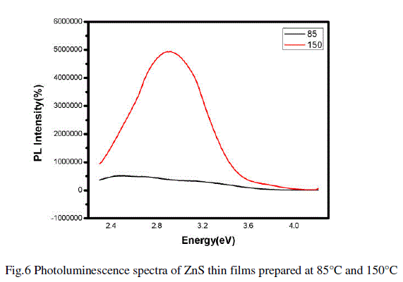 |
| Fig (6) shows the PL spectra of the samples prepared at 85°C and 150°C. The excitation wavelength is 295 nm in each case. PL peaks are found to be broad around 500nm for ZnS film prepared at 85°C and 427 nm for ZnS film prepared at 150°C. The PL spectrum taken from the ZnS film prepared at 150°C depicts a strong intensity than ZnS film prepared at 85°C. ZnS film prepared at 85°C shows blue emission and ZnS film prepared at 150°C shows violet emission. |
V. CONCLUSION |
| ZnS thin films were prepared on glass substrates by the CBD technique. The structure, optical properties, band gap and composition of the samples were determined by XRD, SEM, EDAX, UV-VIS and PL analyses. XRD analysis shows that the samples prepared were in a hexagonal phase. The estimated average grain size was 38 nm for ZnS film deposited at 85°C and 74 nm for ZnS film deposited at 150°C.The SEM micrograph reveals that substrate was well covered. The composition was determined by EDS and it exhibits mainly Zn and S peaks, further confirming that the sample is pure ZnS. From UV results, optical absorption edge is located at 286nm. PL peaks are found to be broad around 500nm for ZnS film prepared at 85°C which shows blue emission and 427 nm for ZnS film prepared at 150°C which shows violet emission. It was found that both structural and optical properties vary with deposition temperatures i.e. 85°C and 150°C. From these studies we are able to optimize the process in order to produce the layer suitable for optical window in solar cells |
References |
|