International Journal of Innovative Research in Science, Engineering and Technology
ISSN ONLINE(2319-8753)PRINT(2347-6710)
ISSN ONLINE(2319-8753)PRINT(2347-6710)
Atulkumar Sojitra1, Arun Nandurbarkar2
|
| Related article at Pubmed, Scholar Google |
Visit for more related articles at International Journal of Innovative Research in Science, Engineering and Technology
This paper describes the Gain boost class–C inverter circuit, which is used in place of OTA (Operational Transconductance Amplifier) block in ΣΔ modulator .The gain boost class-C inverter behaves as a low voltage, subthreshold amplifier and boosts its DC gain for the high precision requirement. First a traditional cascade class-C inverter is presented, another inverter circuit present in this paper is “Gain boost class-C inverter”. It is implemented in 50nm CMOS technology and simulation is done using the LTSpice simulation tool.
Keywords |
| CMOS, cascode inverter, LT-Spice, gain boost class-C inverter. |
INTRODUCTION |
| The continuing feature size scaling in CMOS technology has enabled the digital system to decrease power consumption and lower costs while also increasing reliability. The supply voltages must be scaled along with transistor dimension to maintain the device’s reliability. However, the threshold voltage is not scaled as aggressively as the supply voltage to avoid leakage current in transistors. Therefore, the design of low-voltage analog circuits in the scaled CMOS technology poses significant challenges. Especially, the design of an operational transconductance amplifier (OTA), a key analog building block, has been the main bottleneck in low-voltage analog circuits. Low voltage OTAs have been explored [1]–[2], but the supply voltages of the OTAs are restricted and have reached the limits of further scaling, because they are strictly limited by the input common-mode voltage. |
| A number of design techniques have been investigated to overcome these challenge. Considering the OTA itself, a body-driven OTA and digitally assisted OTAs, have been reported. To remove the need for OTAs, comparator-based [3], time-based [4], and charge-domain [5] circuits have been proposed. A comparator-based circuit is proposed to replace an OTA by a comparator and current sources [3] that remove feedback and stability concerns, but a comparator also has difficulties with low supply voltages. |
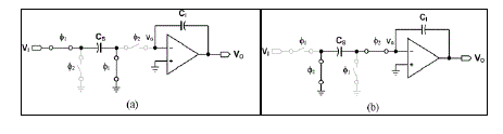 |
| There has been another approach to overcome these problems. It is an inverter-based switched-capacitor (SC) circuit that does not utilize an OTA as an active feedback element. Classically, inverters have been considered to be very simple amplifiers, and are applied to SC circuits [6], [7]. In spite of the limited performance of inverters compared with OTAs, inverters attract attention again [8], [9], because of their ability to operate with very low supply voltages, even when the supply voltage is not large enough to turn on the transistors. Hence, the supply voltage limitation of an OTA is resolved in an inverter-based design. The main objective of this work is to introduce the cascade class-C inverter and the gain boost class-C inverter which can be used in place of the OTA in many different SC (Switched Capacitor) circuits in the CMOS technologies Fig. 1 and Fig. 2. The gain boost class-C inverter is proposed in this paper, which boosts the inerter dc gain to 83 dB in the typical condition |
 |
| This paper is organized into five sections. Section II discuss the inverter as an amplifier. Section III describes the cascode class- C inverter and gain boost class-C inverter and section V gives simulation results of the gain boost class-C inverter. |
II. INVERTER AS AN AMPLIFIER |
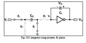
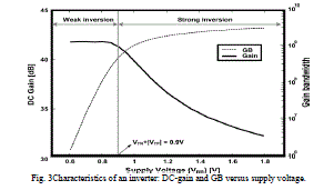
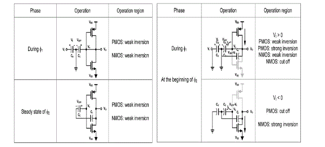
| In SC circuits, the open loop DC-gain of an amplifier determines the accuracy of the charge transfer, while the gain-bandwidth product (GB) of an amplifier determines its operation speed. Fig. 3 shows the DC-gain and GB of a push-pull CMOS inverter with respect to the supply voltage (VDD). The DC-gain of an inverter is maximized in the weak inversion region, whereas the GB of an inverter increases with respect to supply voltage and is saturated as the operating region enters the strong inversion region. To obtain both high DC-gain and wide GB, the inverter should operate at the boundary between the weak and strong inversion regions, which can be realized by using a supply voltage equal to the nominal sum of the NMOS transistor’s threshold voltage, VTN and PMOS transistor’s threshold voltage, VTP. According to the supply voltage, the push-pull inverters can be classified into class-AB or C inverters. When VTN + |VTP |< VDD, the inverter behaves as a class-AB amplifier, while itoperates as a class-C inverter, when VTN + |VTP | >= VDD. If the supply is chosen to be VTN + |VTP |, the inverter-based SC circuit operates as described in Table I. During Φ1, the inverter |
 |
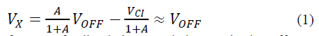 |
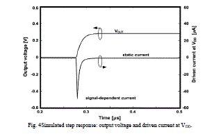
| forms a feedback loop and the VX is the offset voltage as equation (1). At this phase, both transistors operate in the weak inversion region. At the beginning of Φ2, the input node of the inverter is instantaneously changed to VOFF - VI and one of the transistors is biased at a strong inversion region while the other is completely off, depending on the polarity of the input. The charge transfer occurs because of the negative feedback formed through CI. Then, VX gradually returns to VOFF. Once the charge transfer is completed, both of the transistors operate in the weak inversion region again. Therefore, a high slew rate can be obtained with minimum static current because one necessary transistor is operating in the strong inversion region providing high slew rate during transition, and then both transistors operate in the weak inversion region during the steady state providing highDC-gain. Fig. 4 shows the simulated step response of an inverter-based SC integrator when VDD = |VTP |+ VTN. The large signal-dependent current flows only during the transition while the static current is kept very low. When a class-C inverter is used foran amplifier, the settling time can be reduced by about 75% without increasing the static current, because it has a very low short circuit current. |
 |
III. CASCODE AND GAIN BOOST CLASS-C INVERTER |
| As we known, class-C inverter acts as a subthreshold amplifier [10], which is the most important module in the inverter-based design. In this section, the design and application of a gain-boost class-C inverter will be introduced in detail. |
A. Circuit Analysis |
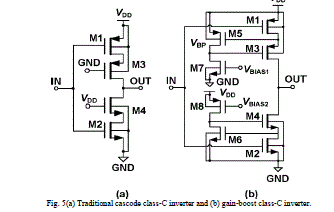
| A traditional cascode class-C inverter is shown in Fig. 5(a), and its nominal supply voltage is 0.8V.To copy with the requirement of the class-C inverter (the supply voltage is slightly lower than the sum of the | VTH | PMOS and NMOS input transistors), both of the input transistors M1 and M2 use regular- VTH core devices. At typical corner, M1 VTH is (-0.4262 V), and M2 VTH is 0.4026 V. However, the inverter dc-gain is insufficient (52dB in our simulation) for some high-resolution applications.Fig.5 (b) adds a gain-boost module to the class-C inverter. The gain-boost module, including transistors from M5 to M8, build up two current-voltage feedback loops together with transistors M3 and M4, respectively. As a result, the output impedance And the dc gain of the gain-boost class-C inverter are enhanced. |
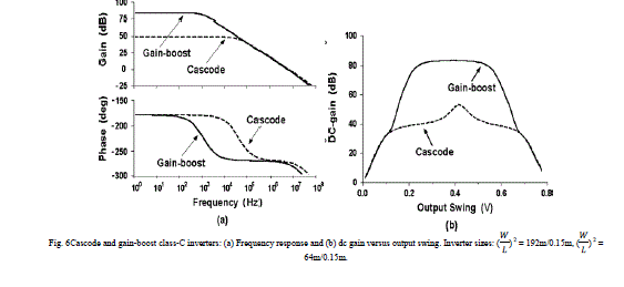
| Fig.6 (a) shows the simulated dc gain and phase margin of the cascode and gain-boost class-C inverters with a 5.75-pF load capacitor. The gain-boost class-C inverter achieves 83-dB dc gain as compared with a 52-dB dc gain in the traditional cascode inverter of the same size at an 0.8-Vsupply.To avoid the loss of output swing, transistors M5 and M6 in the gain- boost inverter employ the low - VTH core devices (The othertransistors use regular- VTH core devices). At a typical corner, |
 ' ' |
| M5 VTH is 0.30 V, and M6 VTH is 0.25 V. As shown in Fig. 6(b), when the inverter output varies from 0.16 to 0.62V, the gainboost inverter keeps a dc gain larger than 60dB, while a worst 37-dB dc gain isobtained by the cascade inverter.In our design, the inverteroutput swing is controlled to be within 0.4V. The gain-boost class-C inverter fully satisfies the dc-gain requirement of 60dB, while the traditional cascade inverter fails. In addition, the gain-boost inverter consumes 34.5 μW at a 0.8-V supply, where the gain-boost modules consume only 3.2 μW (9.3 % power overhead). |
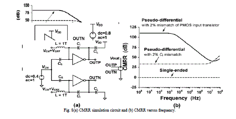
B. PSRR and CMRR |
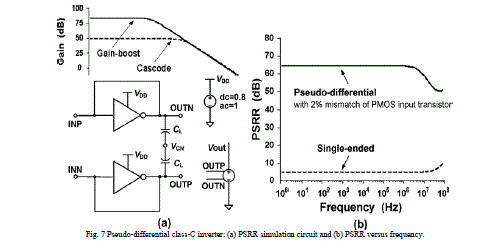
| The single-ended class-C inverter has a relatively high supply voltage gain(ïÿýïÿýïÿýïÿýïÿýïÿý ), leading to a bad PSRR. Fortunately, pseudo-differential structure can improve the inverter PSRR specification. Fig. 7(a) shows the PSRR simulation circuit of pseudo-differential class-C inverter. If the two single-ended branches are ideally the same, their output variations induced by power supply disturbance tend to be cancelled out by each other, achieving an infinitely high PSRR. In other words, the real PSRR of the pseudo-differential inverter depends on mismatch. As seen in Fig.7 (b), the PSRR of the single-ended inverter is only 5.7 dB over audio bandwidth (20–20 kHz). By contrast, the pseudo-differential inverter with 2% transistor mismatch achieves 64.5-dB PSRR, which is comparable with a differential OTA. |
 |
 |
IV.SIMULATION RESULT |
| this section, the functional simulation results of the gain boost class-C inverter have been presented. Functional simulation of gain boost class-C inverter is done in LT-Spice software using 50 nm CMOS technology. |
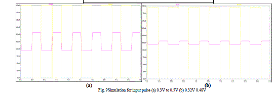
| Table II denotes the short-channel MOSFET parameters for general analog design with a scale factor of 50 nm. In Fig. 5, a proposed Gain boost class– C inverter circuit is shown. The frequency of the analog signal input is varied in the way that the minimal propagation time delay is obtained. For the purpose of functional simulation of the circuit, as shown in fig 9(a) the input of the inverter is set as 0.3V to 0.5V pulse signal and output voltage is 0V to 0.8V, inverted and amplified pulse signal. Here the supply voltage, Vdd is 0.8V. Fig.9 (b) is for pulsed input of 0.38V to 0.42V and the output is 0.025V to 0.792V, inverted and amplified. |
 |
 |
 |
V.CONCLUSION |
| IN THIS PAPER, A GAIN BOOST CLASS-C INVERTER CIRCUIT IS PROPOSED. OTA HAS A PROBLEM WITH THE REQUIREMENT OF HIGHER POWER SUPPLY AND CASCODE CLASS-C INVERTER HAS LOWER DC GAIN WHICH IS LESS SUITABLE FOR DIFFERENT SIGMA DELTA MODULATOR. GAIN BOOST CLASS-C INERTER IS PRESENTED USING 50NM CMOS TECHNOLOGY. THIS ARCHITECTURE ACHIEVES DC GAIN OF 83- DB. AS A FUTURE WORK, WE CAN DESIGN LOW POWER LOW VOLTAGE INVERTER BASED ΣΔ MODULATOR USING THIS INVERTER DESIGN. |
References |
|