International Journal of Innovative Research in Science, Engineering and Technology
ISSN ONLINE(2319-8753)PRINT(2347-6710)
ISSN ONLINE(2319-8753)PRINT(2347-6710)
| Eman M. Nasir Asst. Professor, Physical Dept, College of Science/ University of Baghdad, Jadirya, Baghdad, Iraq |
| Related article at Pubmed, Scholar Google |
Visit for more related articles at International Journal of Innovative Research in Science, Engineering and Technology
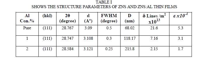
Un doped and doped with Al ZnS thin Films have been fabricated by vacuum evaporation technique under the vacuum of 10-5 Torr on glass substrate at room temperature and with different ratio of Al concentration of thickness (0.8μm). Structure of these films was characterized by X-ray diffraction and Atomic force microscope. The structures of these films grown on glass substrate are in cubic zinc-blende phase and textured along (111) plane. The crystallite size increases from 68.02 to 215.8 nm as the Al concentration increased from pure to 2% Al. The grain size is increase with increasing of Al concentration the surface roughness of the films is decrease with increasing of Al concentration
Keywords |
| ZnS, , thin films, doping, Optical Properties, Structure Properties |
INTRODUCTION |
| Zinc sulphide (ZnS) is an important II–VI semiconducting material with a wide direct band gap of 3.65 eV in the bulk[1] – [5]. This class of new materials has not only provided many unique opportunities but also exhibited novel optical and transport properties, which are potentially useful for technological applications It has potential applications in optoelectronic devices such as blue light emitting diodes, electroluminescent devices and photovoltaic cells [1]-[4], and more recently as n-type window layer heterojunction solar cells. Zinc sulfide has found wide use as a thin film coating in the optical and microelectronic industries. It has high refractive index (2×25 at 632 nm), high effective dielectric constant (9 at 1 MHz) and wide wavelength passband (0×4–13 mm) [2]. There have been various studies on the bulk and thin film characteristics of ZnS including optical and electrical properties.[3]. The optical properties of the prepared film depend strongly on the manufacturing technique. Two of the most important optical properties; refractive index and the extinction coefficient are generally called optical constants. The amount of light that transmitted through thin film material depends on the amount of the reflection and absorption that takes place along the light path [3]. Many growth techniques have been reported to prepare ZnS thin films, such as sputtering , pulsed-laser deposition ,metal organic chemical vapor deposition , electron beam evaporation, photochemical deposition, thermal evaporation, sol-gel processing, co-precipitation and chemical bath deposition [1]-[7]. These doped ZnS semiconductor materials have a wide range of applications in electroluminescence devices, phosphors, light emitting displays, and optical sensors. Doped nanoparticles of dimensions below Bohr diameter exhibit interesting optoelectronic properties due to quantum size effect and are potential candidates for variety of applications. The characteristics and concentrations of dopants are responsible for particular luminescence emission and efficiency of semiconductor nanoparticles. Hence investigation of the role of dopant concentration on optical properties of doped semiconductor nanoparticles is very important from the viewpoints of basic physics as well as applications [7]. Recently, 2D nanostructure P-N junctions have attracted a great deal of attention for their potential applications in photovoltaic device. Zinc sulfide (ZnS) was one of the first semiconductors discovered and is also an important semiconductor material with direct wide band gaps for cubic and hexagonal phases of 3.72 and 3.77 eV, respectively. It has a high absorption coefficient in the visible range of the optical spectrum and reasonably good electrical properties. This property makes ZnS very attractive as an absorber in heterojunction thin-film solar cells. Furthermore, ZnS also offers the advantage of being a nontoxic semiconductor material (without Cd and Pb). A cell with ITO/PEDOT:PSS/P3HT: ZnS/Al structure was showed a very high opencircuit voltage (Voc) value of 1.2 V and a power conversion efficiency of 0.2%. In recent years, ZnS thin films have been grown by a variety of deposition techniques, such as chemical bath deposition, evaporation, and solvothermal method Chemical bath deposition is promising because of its low cost, arbitrary substrate shapes, simplicity, and capability of large area preparation. There are many reports of successful fabrication of ZnS-based heterojunctionsolar cells by the chemical bath deposition method, such as with CIGS used for the n-type emitter layer [8]. In related works Xiaochun et al [6] have been studied the effect of Effects of substrate and annealing temperature on the microstructure, morphology, and optical properties of ZnS films which deposited on glass substrates by an electron beam evaporation. They found that the structure of as-deposited ZnS film exhibiting cubic structure, and the crystallinity is apparently improved with the increase of substrate temperature or annealing temperature. And the average surface grain size and root mean square surface roughness increase with the increase of annealing and substrate temperatures. Ashraf, et al [17] found that the structure of ZnS films which deposited on soda lime glass substrates by a modified close-space sublimation were polycrystalline in natureand having cubic structure oriented only along (111) plan and the crystallinity of films increased with the substrate temperature and the atomic force microscopy data revealed that the films become more uniform and dense with the increase of substrate temperature. Also Shiv et al[9] found that the surface roughness and grain size of the ZnS films increase with increasing TS. In this work pure zinc sulfide and doped with Al thin films are prepared by vacuum evaporation technique. The aim of this work is to preparing ZnS and ZnS:Al thin films and studying the effect of Al concentration on the structure, and morphology properties. |
II. EXPERIMENTAL WORK |
| ZnS and ZnS:AL thin films with different Al concentration of thickness(0.8μm)were prepared by vacuum evaporation technique under lower pressure (10-6 Torr) on glass substrate by using Edward (E306A) coating system. The prepared films have been annealed at 400K The structure of these films grown on glass substrates was examined by a phillips xray diffractometer with copper Kα radiation of the wavelength (λ=1.541 Ao). The surface morphology of the prepared films is investigated by means of atomic force microscopy (AFM) |
III. RESULTS AND DISCUSSION |
| A. XRD Measurements |
| Zinc sulphide exists in sphalerite, cubic and hexagonal forms. The cubic form is stable at room temperature, while the less dense hexagonal form (wurtzite) is stable above 1020oC at atmospheric pressure. However, some authors have observed hexagonal structure for ZnS films and the others observed cubic structure [1-8]. The XRD patterns of films deposited on glass at different Al concentration are shown in Fig. 2. All films shows an intense diffraction peak centered at 28.767 corresponding to the (111) lattice plane of zinc-blende phase (Joint Committee on Powder Diffraction Standard, JCPDS Card No. 77-2100), marked by dotted line and labeled ZB in the pattern. No other diffraction peaks is observed in the pattern which confirms that all is textured along (111) plane. Inset of Fig. 2 shows more clearly the shifting of (111) peak of ZB phase. Similar XRD pattern and structural transformation have been observed [9,10,11]. The Debye-Scherrer formula is used to determine the grain size, and it is increased with increases of Al concentration. The intensity of of (111) cubic plane has been increased, indicating that the degree of preferential orientation toward this direction increased as shown in figure 1. the FWHM of the peak decreased as in Table I, Such crystallinity improvements with increasing the Al concentration have observed by [1-6]. The increasing of intensity with increasing the Al concentration may be permitting better grain growth by maintaining the preference for the (111) plane. The crystallite size increases from 68.02 to 215.8 nm as the Al concentration increased from pure to 2% Al. Similar results are reported by[10,11]. A dislocation is a crystallographic defect, or irregularity, within a crystal structure. The presence of dislocations (δ) strongly influences many of the properties of materials. The dislocation density from the relation was also calculated [5]: |
| δ=1/D2 (1) |
| All the peaks are shifted to higher diffraction angles due to the strain of a high concentration of Al, The micro strain (Ãâ°Ãâº) of films were estimated using the equations |
| ε = βcosθ/4 (2) |
| it is observed from Table I that the grain size increases which intern decreases strain and dislocation density which represents better lattice quality. Similar results are reported by Hasanzadeh et al [5]. Also The grain size of ZnS and ZnS:Al films was approximately estimated by Hall’s method [5] by the equation: |
| (βcosθ/λ)=(1/D)+(2εsinθ/λ) (3) |
| where β is the measured full width at half maximum (FWHM) in radians, θ is the Bragg angle of the diffraction peak, λ is the X-ray wavelength, D is the grain size, ε is the effective residual strain. by plot of β cos θ/λ vs. sin θ/λ for ZnS and ZnS:Al films. ε and D can be estimated from the slope of the straight line and the intercept on the β cos θ/λ axis, respectively. The estimated value for the grain size is 15.87 nm and the effective residual strain is 2.05x10⁻². Similar results are reported by Hasanzadeh et al [5] when they doped with Cu. |
 |
 |
| B. AFM measurements |
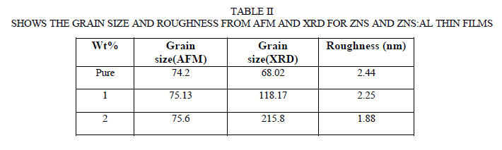
| It is well known that the atomic force microscopy (AFM) is one of the effective ways for the surface analysis due to its high resolution and powerful analysis software The ZnS and ZnS:Al thin films were morphologically characterized using Atomic Force Microscopy (AFM) technique. Also the surface structure of a coating gains more and more importance. In the extreme case of vthin films the surface roughness may be in the order of the film thickness and can influence all film properties such as mechanical, electrical, magnetical or optical properties. Also film morphology, inner structure, texture and crystallinity are strongly connected to roughness evolution. Generally, the reason for the development of roughness during the deposition process is the finite extension of the film forming particles and their random, temporally and spatially uncorrelated impingement at he growth front. The "building blocks" of the film do not necessarily have to be single atoms as it is the case for PVD coatings. They can also be complex molecules (e. g. for organic coatings) multi-particle aggregates as e. g. for cluster deposition or macroscopic aggregates like the ceramic or metallic droplets in the case of thermal spraying. Fig. 2 shows the two and three-dimensional representation of 1090X1090nm area of the ZnS and ZnS:Al thin films with (1%, 2%)Al concentration deposited at room temperatures. It can be seen that films are uniform, densely packed and pinhole free, and it shows that the morphology of these films has larger number of grain size and are homogeneously distributed, which indicates the crystalline nature of the film. Initial visual investigations of the deposited film have shown that they are compact and have good adherence to the substrate. No evidence of cracking observed The grains are made of different sizes varying from 74.2-75.6nm However, the sizes of the grains are noticed to increase as the Al ratio is increased as shown in Table II. Based on AFM image (Fig. 2), the grain density reduced indicating the smaller grains agglomerate together to form larger grains of ZnS and ZnS:Al. On the other hand, the surface roughness and Root Mean Square (RMS) of the films were measured using AFM technique. As in Table II. The surface roughness defined as the standard deviation of the surface height profile from the average height is the most commonly reported measurement of surface roughness [15]. The surface roughness is unavoidable since the grains are grown with different sizes. It can be seen that the surface roughness and RMS values decrease with increasing AL ratio indicating an increase in the grain size As in Table II and Fig. 3., and this is agreement with other literatures[12]-[16]. The histogram of the percentage of ZnS and ZnS:Al. as a function of the grain size are shown in Fig. 3. |
 |
 |
 |
IV.ACKNOWLEDGEMENT |
| The authors wish to acknowledge the support rendered by the laboratories of thin films in physical department, college of science, Baghdad University. |
IV. CONCLUSION |
| Thin films of ZnS and ZnS:Al have been fabricated successfully by vacuum evaporation technique on glass substrate. The XRD shows that the films exhibit crystalline cubic structure oriented in (111) direction. From AFM the morphology of these films has larger number of grain size and are homogeneously distributed and uniform, which indicates the crystalline nature of the film. From the optical measurement the type of transitions is direct and the surface roughness of these films is increase with increasing of Al concentration whereas the grain size increases with increasing of Al concentration. |
References |
|