International Journal of Innovative Research in Computer and Communication Engineering
ISSN ONLINE(2320-9801) PRINT (2320-9798)
ISSN ONLINE(2320-9801) PRINT (2320-9798)
M Premkumar1, P Madhukumar2
|
| Related article at Pubmed, Scholar Google |
Visit for more related articles at International Journal of Innovative Research in Computer and Communication Engineering
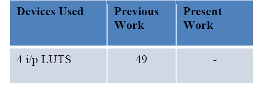
In this paper a new comparator design is proposed by using parallel prefix tree with Zero Detector as decision module. This comparator reduces the power and area requirements. When compared to normal parallel prefix tree based comparator the power is reduced by 225mw because of usage of zero detectors as the decision module. This area and power efficient structure can be used in modern CPU ALUs for improved performance. The simulation results for both parallel prefix tree alone and parallel prefix tree along with Zero detector were compared. Modelsim-Altera 10.1D has been used for simulation of comparators and their power and area analysis was derived by using Xilinx ISE 10.1.
I. INTRODUCTION |
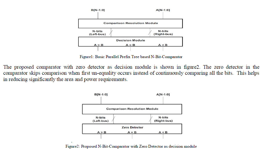
| Comparators form key elements in designing a wide range of applications to support scientific computations, signature analysis and test circuits etc. The basic comparator using parallel prefix tree design is shown in figure1. This structure consists of two basic modules: Comparison resolution module and decision module. |
| The comparison resolution module divides two input N- bit arrays to be compared into two busses namely left bus and right bus each of N bits wide respectively. The decision module in turn decides whether equal, less than or greater than relationship exists between applied inputs for comparison. |
 |
II. OPERATION |
| The comparison proceeds from MSB to LSB by comparing A and B, if they are equal 0 is copied on to left and right buses irrespective of bits compared. The process continues till comparison resolution module finds the first un-equality. In case of first un-equality the current bit compared from A is placed on to the left bus and bit from B is placed in the right bus. The rest of the comparisons were omitted and o s’ were appended for both left and right bus contents. The comparison resolution module therefore structures the left and right buses. In decision module the contents of left bus and right bus are logically or-ed individually to choose whether A>B, A<B or A=B. If both the left bus and right bus contents after performing logic or operation are equal the decision is A=B else the bus on which logical or yields a 1 is considered as the largest value i.e. if logical or results 1 on left bus the decision is A>B otherwise A<B. |
III. COMPARATOR ARCHITECTURE |
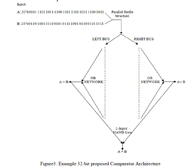
| A 32-bit-comparator using zero detector as decision module was considered. Figure3 shows the comparators architectural overview. In this case A and B are 32-bit inputs 31 down to 0 [N-1 down to 0]. For comparison resolution module A and B are the inputs which are compared from MSB to LSB. Here A31 = 0 and B31=0 i.e., A and B are equal, therefore left bus = right bus=0. Proceeding towards LSB i.e. comparing (MSB-1) bits A30=1 and B30 =1 since A and B are equal left bus =right bus=0. Coming further towards right i.e. comparing (MSB-2) bits A29=0 and B29=1 since A and B are unequal for the first time then left bus=0 and right bus=1. Further comparisons were omitted because A and B are unequal. The rest of the bits in left and right buses were filled with zeros. And further to perform the OR operation for indusial buses and finds comparator result. |
 |
| We partition the structure into five hierarchical prefixing sets as depicted with the associated symbols specific function Whose output serves as input to the next set, until the fifth set produces the output on the left bus and the right bus representation in given below the tables. And Logic gate representations for symbols used comparison module implementation. |
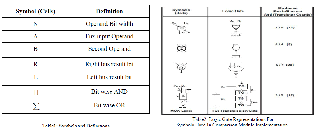 |
| The above symbols are usually used in implementation. Each symbol is represented by the corresponding logic gates. The symbol will perform the operation represented by the logic gate and maximum fan in and fan outs are indicated as 2/4 I.e., the maximum number of inputs are 2 and the maximum number of outputs are 4. These symbols are used to implement the several sets of operations. |
| In comparison resolution module four sets are used and each set performs different gate operations. In set1 the XOR operation is performed with A and B inputs and the output of the gates is D which is 32 down to 0. Set2 perform the NOR operation. The set1 output is given as input for set2 and each gate has 4 inputs with one output. Set3 is similar to set2 (XOR operation). The inverted inputs are applied to NAND gate and its output is also inverted. In decision module set5 performs the multiplexer operation. |
| A new comparator design is proposed by using parallel prefix tree with Zero detector as decision module. Zero detector having less number of gates are used compare to decision module. The zero detector is used to check the left bus and right bus. If all bits are zero or not will be check based on the left bus and right bus results we can find the comparator results. |
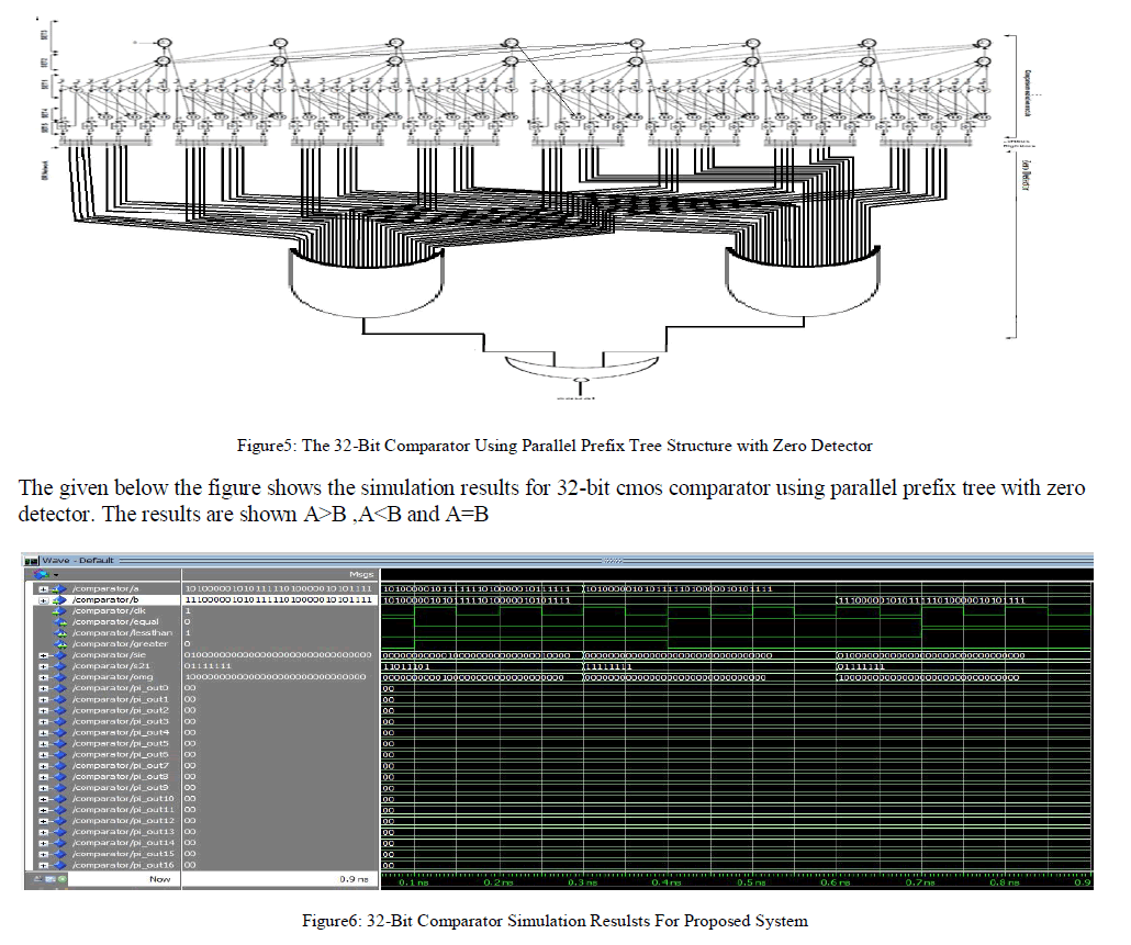
| Given below figure4 shows the designed 32-Bit Scalable Digital CMOS Comparator Using Parallel Prefix Tree. In this section, we detail our comparator’s design which is based on using a novel Parallel Prefix Tree. |
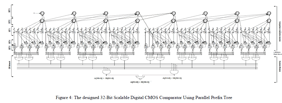 |
| The designed 32-Bit Scalable Digital CMOS Comparator Using Parallel Prefix Tree with Zero Detector as Decision Module is shown in. |
 |
IV. AREA AND POWER EVALUATIONS |
| The 32-bit parallel prefix structure is implemented by using the Xilinx ISE 10.1 and Modelsim-Altera 10.1D. In Xilinx software, we can show design summary |
 |
 |
| i.e., how many LUTs, Flip Flops, slices and gate clocks are used. The figure above shows the device utilization summary. |
| The given below the figure is evaluated power for given clock frequency (50 MHz) for the normal prefix tree structure: |
 |
V. CONCLUSION AND FUTURE WORK |
| In this paper we present a 32-Bit Parallel Prefix Tree Using Zero Detector As Decision Module. This comparator reduces the area and power requirements. Modelsim-Altera 10.1D has been used for simulation of comparators and their power and area analysis was derived by using Xilinx ISE 10.1. In feature work we can include the 64-bit comparator to reduce the power consumption and area using Parallel Prefix Tree with Zero Detector. |