Wireless Sensor Network (WSN) consists of a large amount of low powered nodes which perform tasks like processing, radio transmission-reception, sensing and actuating. To minimize the power consumption in wireless sensor network a dedicated wake-up receiver is used within every sensor node. The wake-up receiver is an additional receiver, which continuously monitors the channel and wakes the rest of the circuit blocks within the node when necessary. In this paper, we carried a brief survey on different wake-up receivers.
Keywords |
| Wake up receiver; low power, VLSI; sensor node; symbol synchronization; WSN |
INTRODUCTION |
| Wireless Sensor Networks (WSNs) consist of very low powered wireless nodes deployed in large number to monitor
the environment or system by measuring physical parameters such as temperature, pressure, humidity etc. Energy
consumption is a critical issue in WSN. These nodes or motes gather information and exchange it with main user
directly or through base station. Sensor nodes are made up of Transducer, Processor, Antenna, Battery and Memory.
Transducer senses the information in environment and converts it as per the need [1]. |
| A. Applications of WSN are: |
| • Sensing of wildfires: To detect drastic changes in temperature or heat, the sensor nodes can be randomly and
densely placed across forest. |
| • Drought prediction: Sensor nodes are deployed in an agricultural field or a plantation to detect the level of
some chemical compounds. The information gathered will be useful in predicting droughts. |
| • Environmental Monitoring: Sensor networks can be used for reliable, update monitoring of the environment.
One example is monitoring the health of bridges and other structures. |
| • Security and Surveillance: This is one of the important applications of wireless sensor networks. Sensors can
be used to improve the safety of roads by providing warnings of approaching cars at intersections. For
identifying and tracking moving entities both imaged or video sensors are useful [2]. |
| The characteristics of a WSN are: large number of nodes, small size nodes, dense deployment and limited power
supply. Therefore, low power design of a sensor node is important. |
WAKE-UP RECEIVER |
| A Wake up receiver monitors the channel continuously. When neighbour nodes send the request wake-up receiver
becomes active. Wake up receiver must have lower power consumption compared to main transceiver [3]. Low power
design of individual analog blocks will certainly reduce the power consumption of a wake-up receiver and this can
enable the use of traditional receivers like heterodyne architecture. However, the main reduction can only come when RF blocks like front-end amplifier are designed for an ultra-low power as they take the highest percentage of the budget
[4].WSN comprises of wake up receiver to detect wireless traffic directed towards receiver of node. It activates it upon
detection. It improves network latency and energy dissipation by maximizing data transceiver sleep time. |
| A novel high gain, high bandwidth and low power envelope detector and low-power asynchronous latching circuitry
use new symbol detection methodology and the corresponding architecture. |
LITERATURE REVIEW ON LOW POWER RECEIVER DESIGN FOR WSN |
| Local Oscillators are used in conventional super- heterodyne receiver, which is not preferable for wake up receiver as
shown in Fig 1. Power budget exceeds itself the power consumption of Local Oscillator of an entire wake up receiver.
Realized in the form of simple ring oscillator used, Local Oscillator work presented [5], which can consume less
power at high cost in LO frequency. Integration takes place over a large bandwidth of circuit noise and consumes extra
power for complex baseband signal processing. In Local Oscillator of 2GHz and buffers are used. The buffers used
dissipate 20μW power. The power dissipated is 10 times less than in LC oscillator. The mixer, IF amplifier and
Envelope detector used in the circuit consumes 8μW, 22μW and 2μW power respectively. It sums up to 52μW power
from the 0.5V power supply. |
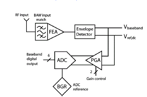
| For wake up receiver a tuned RF architecture has been proposed [3]. It is similar to the fig. 1 but it removes the use of
local oscillator as shown in fig. 2. It uses a complex bit detection algorithm. The signal strength should be sufficiently
high to overcome the forward cut-in voltage. Therefore, envelope detector uses non-linear diode input-output
characteristics. For “always on” wakeup receiver, power consumption is too high to be useful to achieve impressive
sensitivity. Here, 0.5V supply voltage is must. The Front-end Amplifier, PGA, Envelope Detector, Receiver used in the
circuit consumes 48 μW, 2.5 μW, 1 μW and 65 μW power respectively. |
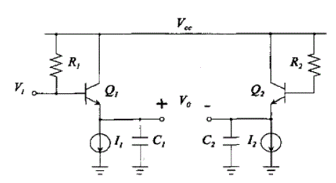
| Input-output characteristics of envelope detectors using non-linear diode are simple and consume low power [6]. A BJT
based high frequency and low power envelope detector as shown in fig.3 was not compatible with CMOS process. So,
BJT is replaced with MOSFET in sub threshold region (as shown in fig.7) but at the cost of a significantly poor gain
and input bandwidth. At the nominal bias current I1=I2=30μA. The bias currents I1 and I2 were varied from 20-50 рA
with no measureable. The largest fractional errors occurred, as expected, at low signal levels. For VI = 50 mV, both
SPICE simulation and measurements gave VO = 20 mV, whereas VO = 18 mV. For VI = 500 mV, SPICE gave VO =
433 mV, measurements at 500 MHz gave VO = 431 mV. |
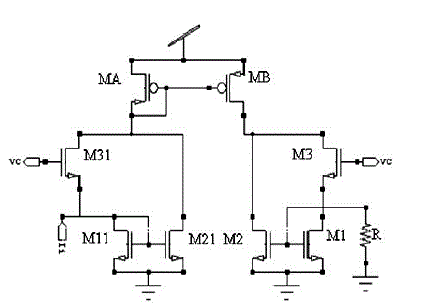
| The current mode full wave rectifier [7] as shown in fig.4 uses the square law of MOSFET to rectify its input. The
unequal gain in positive and the negative half-cycles is the basic problem in this circuit resulting in high ripple in the
baseband signal, which affects the symbol detection process. To achieve high gain and high bandwidth, current mode
detector can be used. The proposed current-mode full-wave rectifier was verified with the 0.8 CMOS process and the
power supply was single3V and the biased voltage was 1.5V. |
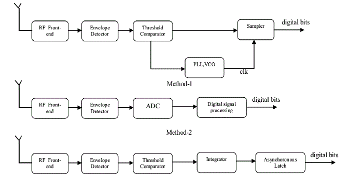
| In [8], various bit encoding and symbol synchronization techniques are described in fig.5. In starting the bit frequency
component is extracted and then using a high gain amplifier clock extract. Incoming data produces nearly accurate
synchronization of clock. So, this type of synchronization is power hungry. |
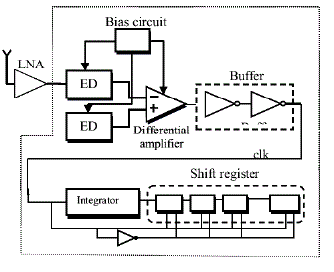
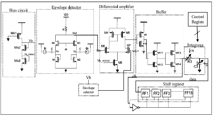
| In fig.6, the use of external clock is avoided during bit encoding scheme. To simplify, the receiver architecture is used
to demodulate On-Off keying for tuned RF architecture. The envelope detector, which takes the input from LNA, down
converts the OOK signal to baseband. The effect of temperature and bias variations is reduced by using a dummy
envelope detector. Action of the inverter stages by buffering the rail to rail level restoration is achieved [9]. |
| For 20% of the bit-period represents symbol ‘0’ and that for 80% of the bit-period represents symbol ‘1’ signal have
carrier presence. Clocking the shift register we use every bit-period of the rail to rail level falling edge is restored
signal. After comparing with particular threshold data is recovered from the level. Wake up signal bits are stored in
shift register and according to the comparison of the bit value WSN wake up followed by necessary action. |
| After demodulation bit period have negative edge at bit boundary. The location of a rising edge depends on bit value.
Clock to negative edged triggered shift register uses output of buffer. Integration of buffered signal is done to recover
data bits which are sampled by shift register. Several D flip-flops connected in master slave configuration consisting of
static transmission-gate latched is realized for the shift register. In [9] process work at 180nm CMOS with supply of
1.8V consumes power 34 μW. |
CONCLUSION |
| Most of the researchers have investigated different architectures for improving the sensitivity and power consumption
of the receiver. A novel technique consisting of envelope detection and low-power synchronization has been presented
for wake-up receivers in WSNs. As there will be an improved implementation of the wake-up receiver in the future,
these comparisons will put the strengths and weaknesses of the wake-up receiver in terms of architecture, circuit
topologies and systems level choices in perspective. Our future work would be to optimize the performance, power and
delay of the wake up receiver. |
Figures at a glance |
 |
 |
 |
| Figure 1 |
Figure 2 |
Figure 3 |
|
 |
 |
 |
| Figure 4 |
Figure 5 |
Figure 6 |
|
References
- Jamal N.Al-Karaki and Ahmed E. Kamal, “Routing techniques in wireless sensor networks: a survey”, wireless communications, IEEE,Vol.11, pp. 1-36, December 2004.
- NeetuKumari, Nikita Patel, SatyajitAnandand ParthaPratim Bhattacharya “Designing Low Power Wireless Sensor Network: A Survey”, in International Journal of Advanced Research in Electrical, Electronics and Instrumentation Engineering , Vol. 2, Issue 9 , pp. 4447-4456, September 2013.
- N. Pletcher, S. Gambini, J. Rabaey, “A 65 ÃâõW, 1.9GHz RF to Digital Baseband Wakeup Receiver for Wireless Sensor Nodes”, Proc. IEEE Custom Integrated Circuits Conf. (CICC), pp. 539-542, September 2007.
- FikreTsigabuGebreyohannes, “Design of an Ultra-Low Power Wake-Up Receiver in 130nm CMOS Technology”, Master's Thesis performed in Electronic Systems, pp. 1-8811, June 2012.
- N. M. Pletcher, S. Gambini, J. M. Rabaey, “A 2GHz 52ÃâõW Wake-Up Receiver with -72dBm Sensitivity Using Uncertain-IF Architecture”, ISSCC Dig. Tech. Papers, pp. 524-633, February 2008.
- R. G. Meyer, “Low-Power Monolithic RF Peak Detector Analysis,” IEEE J. Solid-State Circuits, vol. 30, no. 1, Jan. 1995. IEEE JOURNAL OF SOLID-STATE CIRCUITS, Vol.30, Issue 1, pp. 65-67, January 1995..
- C. C. Chang, S. I. Liu, “Current-Mode Full-Wave Rectifier and Vector Summation Circuit”, Electronic Letters, Vol.36, Issue 19, pp. 1599-1600, September 2000.
- B. Sklar, “Digital Communications Fundamentals and Applications”, 2nd Ed., Prentice Hall, pp. 1-1079, 2001.
- Deepak Kumar Meher, ArunkumarSalimath, AchintyaHalder, “An Ultra-low Power Symbol Detection Methodology and Its Circuit Implementation for a Wake-up Receiver in Wireless Sensor Nodes” 25th International Conference on VLSI Design, pp. 274-279, 2012.
|