In this paper, an antenna has been designed and implemented for wireless sensor node. The antenna element of the proposed node is based on Omni directional PCB (printed circuit board) patch antenna. It uses meandering connecting strip which is optimized to have frequency band operation, between 2.40 to 2.49 GHz for |S11| ≤ -10 dB. This work is a part of development of the wireless sensor node for a specific application. We have designed a dipole antenna suitable for the specific application using FR-4 epoxy glass laminate material, and have presented the simulated result obtained from NEC 4.0V simulation tool. This design has a better power handling capacity. Further, we have implemented this for the wireless sensor node as well.
Keywords |
| WSN Antenna, Patch Antenna, Antenna Design, PCBantenna |
INTRODUCTION |
| The antenna is a key constituent in a wirelesscommunication system. The main objective of an antenna is
totransform electrical signals into RF electromagnetic waves.The electromagnetic waves are then propagated into free
space(transmit mode) and are transformed into electrical signals(receive mode). A characteristic antenna is basically an
air coreinductor of definite wavelength. The AC current through aninductor or conductor lags the voltage by
approximately 90degrees so the maximum power is delivered at ¼ wavelengths.If wavelength is λ then the λ/2 dipole
produces most power atthe ends of the antenna with little power in the centre of theantenna. The other similar work
with different geometry andapplication of antenna are cited in articles [1,4]. |
DESIGN THEORY |
| There are diverse types of antenna for the better outputpower, sensitivity and antenna gain. Reducing its frequency
bya factor of 2 doubles its range (line of sight). Lowering theoperating frequency also signifies that the antenna
increases insize. When choosing the operating frequency for a radiodesign, the available board space must also
accommodate theantenna. So the choice of antenna, and the size available shouldbe considered at an early stage in the
design. |
 |
| Moritz Von Jacobi’s maximum power theory states thatmaximum power transfer happens when the source
resistanceequals the load resistance. For complex impedances, themaximum power delivered from a transmission line
withimpedance Z0 to an antenna with impedance is Za, It isimportant that Z0 is properly matched to Za. If a signal
withamplitude VIN is sent in to the transmission line, then only apart of the incident wave will be transmitted to the
antenna if.Z0 is not properly matched to Za then it is. |
 |
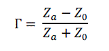
| The complex reflection coefficient (Γ) is defined as theratio of the reflected waves’ amplitude to the amplitude of
theincident wave. Γ can be calculated from the impedance of thetransmission line and the impedance of the antenna, as
shownin the equation: |
 |
| The reflection coefficient is zero if the transmission lineimpedance is the complex conjugate of the antenna
impedance.Thus if then the antenna is perfectly matched to thetransmission line and all the applied power is
delivered to theantenna. Antenna matching typically uses both; the ReturnLoss and the Voltage Standing Wave Ratio
(VSWR)terminology. VSWR is the ratio of the maximum output (Input+ Γ) to the minimum waveform (Input – Γ)
shown in followingequation. This means that a specific geometry can be madeabout half the size of a required patch
(area of interest). Theinput impedance levels have much the same dependence as thatfor the required patch. By
selecting the required position toobtain as good a match as possible to with a connector and theVSWR bandwidth was
computed. It can be seen that thebandwidth varies if there is change in patch size [2]. |
 |
| The power ratio of the reflected wave to the incident waveis called Return Loss. This indicates as to by how
manydecibels is the reflected wave power below the incident wavereturn loss for the same port. It can be seen that a
very goodimpedance match (|S11| less than -20 db) is achieved for eachdesired level of miniaturization [3]. |
 |
| Antenna design, VSWR and Return Loss are measures withwhich we can find out how well the antenna functions.
Themismatching of the antenna is one of the largest factors thatreduce the total RF link budget. To avoid
unnecessarymismatch losses, it is recommended to add a pi-matchingnetwork so that the antenna can always be
matched. If theantenna design is adequately matched then it just takes onezero ohm resistor or DC block cap to be
inserted into the π_matchingnetwork. There are a numerous issues to considerwhen selecting the antenna: |
| • Antenna placement |
| • Ground planes for ¼ wavelength antennas |
| • Undesired magnetic fields on PCB |
| • Antenna mismatch (VSWR) |
| • Objects that alter or disrupt Line of Sight (LOS) |
| • Antenna gain characteristics |
| • Antenna bandwidth |
| • Antenna Radiation Efficiency |
PROPOSED DESIGN DIMENSION |
| There are several antenna types to choose from whiledeciding what kind of antenna to be used in an RF
product.Size, cost and performance are the most vital factors to be keptin mind at the time of choosing an antenna.
The three mostcommonly used antenna types for short range devices are; PCBantennas, chip antennas and Segment
antennas, all of whichhave their own pros and cons. Here, we have focused on PCBantenna since they are very cost
effective, easy to implementand have better performance at more than 868 MHz. Also, asmall size PCB antenna at
high frequencies can be design asper the application requirement. |
| The antennas discussed in this paper are for the license freeworld wide band 2.4000 GHz - 2.4900 GHz band
and the allthe standard frequency bands at sub 1 GHz. For the sub 1 GHzbands; there is usually a “low“ sub 1 GHz
band and a “high”sub 1 GHz band. Our ambition is to provide excellent antennadesigns for our application with
Omani directional radiation. |
| Total area covered by the antenna is shown in fig 1 andphysical dimension on each strip of antenna are
described in fig2, Total length of track c/c = (270+55x6+150x6+145) = 1645mils. The width of track is 20 mils and
its spread area is260x280, The length of Ltips = 165 mils (Segment D strip infig 2), PCB thickness is 31 mils, Cap
track (segment E) is 273mils, The capacitance track below segment is 273 mils forthickness of PCB 0.08mm. This
assembly can maintain thecapacitance of around 0,22pF. The material used for the PCB isFR-4 epoxy glass which
is laminated with HTE Copper ofthickness of 0.0032 inches ± 10%.Aim of the proposed algorithm is to maximize
the network life by minimizing the total transmission energy using energy efficient routes to transmit the packet.
The proposed algorithm is consists of three main steps. |
| After carrying out the design calculations of the proposedantenna we reach Fig 2, which consists of 16 segments.
Thedimension details for creating this image in simulation softwareare given in the following table in geometrical
absolutecoordinate system. |
SIMULATION RESULTS |
| As an outcome of our data, we get the simulated antenna image similar to Fig 3. This antenna design falls in a dipole
antenna category with loading effect. In this antenna feed is offset, but it is not a monopole structure unlike most of the
antenna. It is wire base meander based antenna. In order to reduce the vertical height, we have applied the meander
shape as loading. The power handling capacity will be up to +60dBm as shown in Fig 5. |
| This fig 4 shows the 3D pattern of the field strength & inclination. This fig also shows horizontal plane having
directivity, “eight shapes” pattern is obtained due to dipole structure. This shows f/b ratio optimization but is not our focus. It shows impedance is 35 ohm. The co-polarize pattern is around -12db down. The entire antenna factor is better
the other tried samples and pattern This fig 5 shows the max gain is 1.6 dB in elevation plane the result obtained from the simulation tool which is based
on SLOVER IS MOM. The fig 6 shows the Omni directional pattern which obtained in elevation plane. The pattern
axis is shifted in H plane, which is due to loading. |
IMPLEMENTATION RESULTS |
| After analyzing the result of above work we fabricated the same patch antenna on the PCB of the wireless sensor
node* and got the result on lab successfully are going to test on real tile field soon along with the application need and
required rules of communication. Due to the loading the impedance is modified from 73 ohm, the reactive part is too
high to suppress the antenna efficiency .the antenna factor is low. To match this specification impedance matching
circuit is employed. The PCB layout of this antenna is shown in fig 7 and the impedance marching circuit is shown in
fig 8. The vales of the capacitanceand inductance can be selected as per the actual impedanceafter fabrication of PCB
and require gain. |
CONCLUSION AND FUTURE WORK |
| From above result discussion we would like to state that thePCB bases antenna is better cost effective solution for
wirelesssensor node for a typical application. It shows the betterperformance than inverted F antenna [1] |
| |
Tables at a glance |
 |
| Table 1 |
|
| |
Figures at a glance |
 |
 |
 |
 |
| Figure 1 |
Figure 2 |
Figure 3 |
Figure 4 |
 |
 |
 |
 |
| Figure 5 |
Figure 6 |
Figure 7 |
Figure 8 |
|
| |
References |
- AnjumC.Soras, M. Karaboikis, G. Tsachtsiris and V. Makios, "Analysis and design of an inverted-F antenna printed on a PCMCIA card for the 2.4GHz ISM band," IEEE Antennas and propagation magazine, vol.44, no.1, pp.37-43, February 2002
- S. A. Bokhari , J. F. Zuercher , J. R. Mosig and F. E. Gardiol "A small microstrip patch antenna with a convenient tuning option", IEEE Trans. Antennas Propag., vol. 44, no. 11, pp.1521 -1528 1996
- Ouedraogo, R.O.; Rothwell, E.J.; Diaz, A.R.; Fuchi, K.; Temme, A. "Miniaturization of Patch Antennas Using a Metamaterial-Inspired Technique", Antennas and Propagation, IEEE Transactions on, On page(s): 2175 - 2182 Volume: 60, Issue: 5, May 2012.
- Matsuoka, H.; Seto, I.; Sekiguchi, T.; Yoshida, H.; Tsujimura, A.; Namekata, M. "Development of a PC card using planar antennas for wireless LAN on 2.4/5 GHz bands", Wireless Communications and Networking Conference, 2005 IEEE, On page(s): 573 - 577 Vol. 1 Volume: 1, 13-17 March 2005.
|