Keywords
|
| Application-specific integrated circuit (ASIC), area-efficient, CSLA, low power |
INTRODUCTION
|
| Design of area- and power-efficient high-speed data path logic systems are one of the most ubstantial areas of research in VLSI system design. In digital adders, the speed of addition is limited by the time required to propagate a carry through the adder. The sum for each bit position in an elementary adder is generated sequentially only after the previous bit position has been summed and a carry propagated into the next position. The CSLA is used in many computational systems to alleviate the problem of carry propagation delay by independently generating multiple carries and then select a carry to generate the sum [1]. However, the CSLA is not area efficient because it uses multiple pairs of Ripple Carry Adders (RCA) to generate partial sum and carry by considering carry input Cin=0 and Cin=1, then the final sum and carry are selected by the multiplexers (mux). The basic idea of this work is to use Binary to Excess-1 Converter (BEC) instead of RCA with Cin=1 in the regular CSLA to achieve lower area and power consumption [2]–[4]. The main advantage of this BEC logic comes from the lesser number of logic gates than the n-bit Full Adder (FA) structure. In this paper, we proposed the modified BEC SQRT CSLA architecture. |
| In this paper [1], that the problem of carry propagation delay is overcome by independently generating multiple radix carries and using this carries to select between simultaneously generated sums. In this adder system, the addend and augends are divided into sub addend and sub augends sections that are added twice to produce two sub sums. One addition is done with a carry digit forced into each section, and the other addition combines the operands without the forced carry digit. The selection of the correct, or true, sub sum from each of the adder sections depends upon whether or not there actually is a carry into that adder section. |
| In this paper [2], the design and implementation of a generic fast asynchronous Hybrid Kogge-Stone Structure Carry Select based Adder (HKSS-CSA) is described in detail and its application in the design of asynchronous Double Precision Floating-Point Adder (DPFPA) is presented and the improved latency performance it provides is discussed. A detailed analysis in terms of maximum combinational delay, number of logic levels and logic resources used by both these adders is provided. The proposed HKSS-CSA adder’s performance is compared with a generic reference Carry Look- Ahead Adder (CLA) in terms of the parameters. |
| In this paper [3], that instead of using dual Ripple Carry Adder a Carry Select Adder scheme using an add one circuit to replace one RCA adder requires 29.2% fewer transistors with a speed penalty of 5.9% for bit length 17 = 64. If speed is crucial for this 64bit adder, then two of the original carry-select adder blocks can be substituted by the proposed scheme with area saving and the same speed. |
| In this paper [4], they introduced a scheme to generate carry bits with block carry in 1 from the carries of a block with block carry in 0. This paper introduces a new reduced-area carry-select scheme where the second copy of the carrychain is substituted by an ‘or’ gate per bit position. Replacing the ripple-carry blocks with parallel-prefix blocks results in a select-prefix adder, which has a slightly better area and time than a parallel-prefix adder. |
| In this paper [5], an adder is introduced to operates with low power and occupies lower area in comparison to conventional CSLA circuit due to using a first zero finder circuit. Besides by three basic changes in the critical path of adder, speed is improved considerably. First of all we used a high speed compact CSLA as partial adder in each block, then a block carry generator (BCG) circuit is used for faster carry propagation and finally we replaced multiplexer gate with a XNOR gate. For designing a fast CSLA, we used combination of conventional CMOS (C-CMOS) and Transmission Gate (TG) logic styles. Also using Complementary Pass-transistor Logic (CPL), due to lower parasitic capacitance, is faster. |
| In this paper [6], an Efficient Novel carry select adder works according to the BEC technique. In this type of Adder, the block of Ripple Carry Adder with input carry as 1 has been replaced with a block of Binary to Excess-1 converter (BEC). The BEC stage is constructed by NMOS stage and also acts as a pass gate. For n-bit ripple carry adder, n+1 bit of Binary to Excess-1 converter is used. This is done in order to reduce the area and power requirement of the previous Carry Select Adder. |
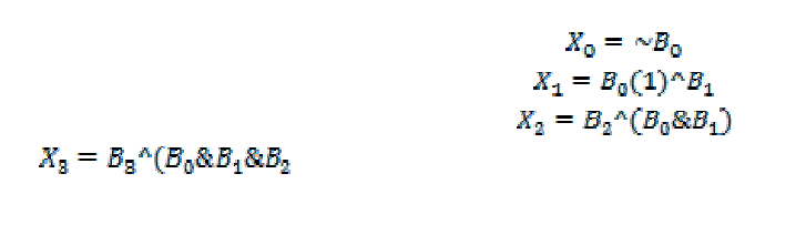
In this paper [7], a BEC technique is introduced, which is a simple and efficient gate level modification to significantly reduce the area of SQRT CSLA. The main idea of this work is to use BEC instead of the RCA with Cin =1 in order to reduce the area and power consumption of the regular CSLA. To replace the n-bit RCA, an n+1-bit BEC is required. One input of the 8:4 mux gets as it input (B3, B2, B1, and B0) and another input of the mux is the BEC output. This produces the two possible partial results in parallel and the mux is used to select either the BEC output or the direct inputs according to the control signal  . The importance of the BEC logic stems from the large silicon area reduction when the CSLA with large number of bits are designed. . The importance of the BEC logic stems from the large silicon area reduction when the CSLA with large number of bits are designed. |
| In this paper [8], they introduced a multiplexer based add one circuit which is used to reduce the area with negligible speed penalty. The proposed 64 bit carry-select adder requires 42% fewer transistors than the conventional carryselect adder. The complement scheme by Chang was used for designing an add-one circuit. The results of two RCAs with= 0 and = 1, are manipulated respectively. The complement scheme states that adding one generates Sf bit by inverting each S bit starting from the least significant bit until the first zero is found. This complement scheme can be implemented using multiplexers. |
| In this paper [9], an area efficient Square-root CSLA (SQRT CSLA) scheme based on a new first zero detection logic. For CSLA with large operand, the longest RCA adder may contain a long carry chain. Therefore, a buffer should be inserted between every two pass transistors to restore the drive and logic level of the decaying signal strength along cascaded chain of pass transistors. To simply the layout and lower the transistor count for further interconnect and logic area reduction, we propose a new add-one scheme, which neither employs single inverter buffers and uses only MUX to substitute exclusive NOR gates along with MUX. |
| In this paper [10], a modified CSLA is designed in different stages and it reduces the area. CSLA is used in many computational systems to relieve the problem of carry propagation delay by independently generating multiple carries and then select a carry to generate the sum ‘1’. However, the CSLA is not area efficient because it uses multiple pairs of RCA to generate partial sum and carry by considering carry in 0 and carry in 1, then the final sum and carry are selected by the multiplexers (mux). Instead of using two separate adders in conventional CSA, one for the Cs =1 and another for the Cs=0. One adder is used to reduce the area and power consumption. Each of the two additions is performed in one clock cycle. |
| The details of the BEC logic are discussed in Section II. This brief is structured as follows. Section II deals with the delay and area evaluation methodology of the basic adder blocks. Section III presents the detailed structure and the function of the modified BEC logic. The SQRT CSLA has been chosen for comparison with the proposed design as it has a more balanced delay, and requires lower power and area [5], [6]. The delay and area evaluation methodology of the regular and modified SQRT CSLA are presented in Sections II, III and IV respectively. Finally, the work is concluded in Section V. |
EXISTING SYSTEM
|
| Carry Select Adder (CSLA) |
| In RCA every full adder has to wait for the incoming carry before an outgoing carry is generated. One way to get around this linear dependency is to anticipate both possible values of the carry input i.e. 0 and 1 and evaluate the result in advance. Once the real value of the carry is known the result can be easily selected with the help of a simple multiplexer stage. |
| A 16-bit CSLA is constructed by dividing into 4 stages i.e. N=16 total number of bits, M=4 number of bits per stage, (N/M = 4) and chaining such four equal length blocks as shown in Figure 1.6. CSA has less delay as compared to RCA due to the anticipation of both possible values of in advance, and as the multiplexers is used for the selection of , so the area increases as compared to RCA. The propagation time through the Carry Select Adder is calculated using following mathematical equation: |
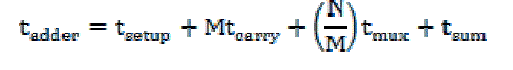 |
Where, is delay of the setup stage to produce propagate and generate signals, is delay of the setup stage to produce propagate and generate signals, is the time taken by the carry to ripple through a length of the stage M , is the time taken by the carry to ripple through a length of the stage M ,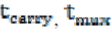 is the delay of the multiplexer stage and is is the delay of the multiplexer stage and is sum of time. sum of time. |
| The existing system uses BEC instead of RCA with carry in 1 in the regular CSLA to achieve lower area. With an efficient design of an add-one circuit, the power and area of CSA can be reduced. But the XOR function in BEC consists of five gates according to the previous design. The Figure 2 shows the existing BEC circuit and the Figure 3 shows the existing XOR function. |
 |
PROPOSED SYSTEM
|
| Above diagram clearly shows the modified BEC structure of the SQRT CSLA. It has reduced area compare than basic BEC structure of the SQRT CSLA. Below table indicates the area reduction of modified BEC structure of SQRT CSLA. |
| MODIFIED CARRY SELECT ADDER (MCSA) DESIGN |
| A Modified Carry Select-Adder (MCSA) design is proposed, which make use of single RCA and Binary to Excess-1 Converter (BEC) instead of using dual RCAs to reduce area and power consumption with small speed penalty. The reason for area reduction is that, the number of logic gates used to design a BEC is less than the number of logic gates used for a RCA design. Thus, the importance of BEC logic comes from the large silicon area reduction when designing Modified Carry Select Adder for large number of bits. The Modified Carry Select Adder architecture for 16-bit is shown in Figure 5. |
| As to replace the N bit RCA, an N+1 bit BEC is used, so in above designed architecture of MCSA, the 4-bit RCA is used in each block and thus the BEC used is of 5-bit wide. In the similar way MCSA architectures are designed for 8-bit, 16-bit, 32-bit and 64-bit. |
| The circuit in BEC are modified by using simple AOI logic by reducing the gates in XOR by simplifying the Boolean logic. The total number of gates reduced is 42 than the conventional one. Conventional CSA is still areaconsuming due to the dual ripple carry adder structure. The metrics for measurement of performance of a circuit are area, power and delay. So, after designing MCSA for 8-bit, 16-bit, 32-bit and 64-bit its area, power and delay are analyzed. The results so obtained are then compared with the results of conventional CSA. |
RESULTS AND DISCUSSIONS
|
| MICROWIND |
| Tool which is chosen to simulate this scheme is microwind & DSch Version2.DSCH stands for Digital Schematic. |
| 1. DSch2: |
| The DSCH2 is a logic editor and simulator.DSCH2 is used to validate the architecture of logic circuit before the microelectronics design is started.DSCH2 provides user friendly environment for hierarchical logic design and simulation with delay analysis which allows the design and validation of complex logic structures. A key innovative future is the possibility to estimate the power consumption of the circuit. |
| 2. MICROWIND: |
| MICROWIND2 Program allows the student to design and simulate an integrated circuit at physical description level. The package contains the library of common logic and analog ICs to view and simulate.MICROWIND2 includes all the commands for a mask editor as well as original tools never gathered before in a single module. Gain of this tool is access the circuit simulation by pressing a single key. The electric extraction of the circuit is automatically performed and the analog simulator produces voltage and current curves immediately. |
| MICROWIND tool simulates the digital schematic diagram of basic BEC SQRT CSLA structure and modified BEC SQRT CSLA structure. This simulation provides area and power consumption results. Below table indicates the area and power consumption results of basic BEC and modified BEC SQRT CSLA. |
CONCLUSION
|
| The Proposed work provides an efficient adder for arithmetic operations by using the Modified Carry Select Adder. Comparing it to the conventional design it has an advantage of area reduction by less number of gates and low power circuit. Considerably the delay is also reduced by modified CSLA. The gate counts are reduced by modifying the Binary to Excess One Converter unit and the Ripple Carry Adder unit by simplifying using AOI logic. The proposed CSLA is implemented for different Word sizes. The proposed design may be suitable for low power applications such as Filter design, Multipliers and digital signal processing. In the future work the Extension of word size up to 128-bit can be designed and implemented in FPGA Board design. Then the CSLA can be implemented in Multiplier and Filter applications and its speed of operation is evaluated. |
Tables at a glance
|
 |
|
|
|
| Table 1 |
Table 2 |
Table 3 |
Table 4 |
|
Figures at a glance
|
 |
 |
 |
 |
 |
| Figure 1 |
Figure 2 |
Figure 3 |
Figure 4 |
Figure 5 |
|
References
|
- AkhileshTyagi, (1993), “A Reduced-Area Scheme for Carry-Select Adders”, IEEE Transactions on Computers, Vol.42, No.10, pp.1163-1170.
- Bedrij.J.O, (1962), “Carry-select adder”, IRE Trans. Electron. Computer, pp.340-341.
- Ceiang.Y.T and Hsiao.M.J, (1998), “Carry-select adder using single ripple Carry adder”, Electron. Lett, vol. 34, no. 22, pp. 2101–2103, October.
- Chang, C. H. and Gu.J. (2005), “An Area Efficient 64-Bit Square Root Carry-Select Adder for Low Power Applications”, in Proc. IEEE Int. Symp. Circuits Syst., Vol.4, pp. 4082–4085.
- Edison A.J and Manikandababu.C.S, (2012), “An Efficient CSLA Architecture for VLSI Hardware Implementation”, International Journal for Mechanical and Industrial Engineering, Vol. 2.Issue 5.
- Kim.Y and Kim.L.S, (2001), “64-bit carry-select adder with reduced area”, Electron. Lett. vol. 37, no. 10, pp. 614–615, May.
- Priya.R and SenthilKumar.J, (2013),” Implementation and Comparison of Effective Area Efficient Architectures for CSLA”, ICECCN 978-1- 4673-5036-5/13.
- Padma Devi, (1998), “Improved Carry Select Adder with Reduced Area and Low Power Consumption”, International Journal of Computer Applications, Vol.3, No.4, pp. 14.
- Ramkumar, B. and Harish M Kittur, (2012), “Low Power and Area Efficient Carry Select Adder”, IEEE Transactions on Very Large Scale Integration (VLSI) Systems, pp.1-5.
- Ramkumar.B, (2010), “ASIC implementation of modified faster carry save adder,” Eur. J. Sci. Res., vol. 42, no. 1, pp.53–58.
|