International Journal of Advanced Research in Electrical, Electronics and Instrumentation Engineering
ISSN ONLINE(2278-8875) PRINT (2320-3765)
ISSN ONLINE(2278-8875) PRINT (2320-3765)
Subitha. S1, Mrs. Jayarama Pradeep M.E.,(Ph.D) 2
|
| Related article at Pubmed, Scholar Google |
Visit for more related articles at International Journal of Advanced Research in Electrical, Electronics and Instrumentation Engineering
Abstract- In this paper, a zero voltage full bridge dc-dc converter pulse width modulation and capacitive output filter is presented. The application for this second stage dc-dc converter is a two stage on-board charger for a plug in hybrid electric battery charging. For this application the design objective is to reduce the cost in order to minimize the charger size, charging time and the amount and cost of electricity drawn from the utility and to achieve high efficiency. A converter operation is presented with results. In comparison to full bridge with an LC output filter, the proposed converter reduces the reverse recovery loses in the secondary rectifier diodes, enabling the high switching frequency. Experimental results are presented in this paper. The peak efficiency 92% is achieved by using the proposed converter. Index Terms- DC-DC converter, plug-in hybrid electrical vehicle (PHEV), capacitive output filter, resonant converters, zero voltage switching (ZVS).
Index Terms |
| DC-DC converter, plug-in hybrid electrical vehicle (PHEV), capacitive output filter, resonant converters, zero voltage switching (ZVS). |
INTRODUCTION |
| A PLUG-IN hybrid electric vehicle (PHEV) is a hybrid electric vehicle which utilizes rechargeable batteries that can be restored to full charge by connecting a plug to an external electric power source. In recent years, PHEV motor drive and energy storage technology have developed at a rapid rate in response to expected market demand for PHEV’s. Battery chargers are another important key components required for the emergence and acceptance of PHEV’s. Mostly for PHEV applications, on-board chargers are used. |
| Common charger power architecture includes an ac–dc converter with power factor correction (PFC) [1]–[7] followed by an isolated dc–dc converter. Galvanic isolation is required in all on-board battery chargers in order to meet the double fault protection for the PHEV user safety [8]– [10]. High efficiency fullbridge dc–dc converter solutions have been proposed that are potential candidates for the isolated dc–dc converter in a PHEV charger [11]–[27]. The phaseshifted zero voltage switching(ZVS) pulse width modulated (PWM) dc-to-dc full-bridge converter was presented in [11]–[13]. ZVS for the switches is realized by using the leakage inductance of the transformer in addition to an external inductor and the output capacitance of the switch. |
| Although various improvements have been suggested for this converter, including [14]–[23], these solutions increase the component count and suffer from one or more disadvantages including, a limited ZVS range, high voltage ringing on the secondary side rectifier diodes, or duty cycle loss. The wide ZVS range of operation is discussed in [15], [20]–[22]. The high voltage ringing on the secondary side rectifier diodes is addressed in [16], [18], [19] and [23]– [27]. Duty cycle loss is reviewed in [17]. A new complementary gating scheme for the full-bridge dc-to-dc PWM converter is presented in [28]. This gating scheme requires an additional zero voltage transition circuit to achieve ZVS for all the switches for a wide variation in the load current. Current fed topologies with capacitive output filter inherently minimize diode rectifier ringing since the transformer leakage inductance is effectively placed in series with the supply side inductor [29]–[34]. In addition, high efficiency can be achieved with ZVS, in particular the trailing edge PWM full-bridge gating scheme proposed in [35] is an attractive solution to achieve ZVS. |
| In this paper, a novel PWM ZVS full-bridge dc– dc converter with the trailing edge pulse width modulation and capacitive output filter is presented. The paper is organized as follows: section II presents the converter operating modes. Design procedure is provided in Section III, followed by simulation results in Section IV. The conclusions are presented in Section V. |
OPERATING PRINCIPLES |
| The proposed ZVS full-bridge converter topology is illustrated in Fig. 1. The converter primary side circuit consists of a full-bridge inverter. The lower switches (Q3 and Q4) are driven at a fixed 50% duty cycle and the upper switches (Q1 and Q2) are PWM on the trailing edge [35].Although the proposed converter can operate in either discontinuous conduction mode (DCM) [33], boundary conduction mode (BCM), or continuous conduction mode (CCM), only the DCM and BCM modes are desirable, as discussed in section III. |
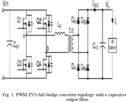 |
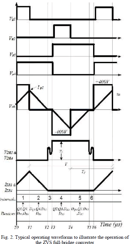
| This converter has six operating intervals. The operating intervals are determined by the ON/OFF states of the four primary switches. Detailed operating waveforms are provided in Fig 2. In the analysis that follows, the power semiconductor switches have been modelled with parallel diodes and parasitic capacitances. The output rectifiers are considered ideal and the external resonant inductor also includes the transformer leakage inductance. |
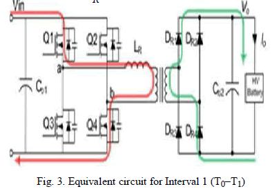
A.Interval 1 (T0−T1) |
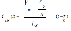
| Referring to Figs 2, during Interval 1 (T0–T1), switches Q1 and Q4 are ON and Q2 and Q3 are OFF. The primary current flows through Q1, resonant inductor LR, transformer primary and Q4, as illustrated in Fig. 5. The rate of rise of the current (di/dt) through LR is proportional to the difference between the input voltage Vin and the output voltage V0 . During this mode power flows to the output through rectifier diodes DR1 and DR4 and also energy is stored in LR. The resonant inductor current iLR (t) using initial condition iLR (0) = 0 is given by |
 |
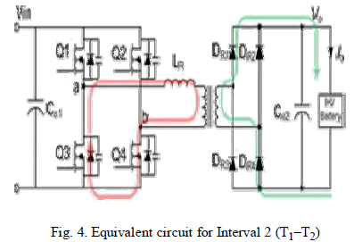
B. Interval 2 (T1–T2) |
| Referring to Fig. 2, interval 2 begins after switch Q1 turns OFF. Since the current flowing in the primary side cannot be interrupted instantaneously, it finds an alternate path and flows through the parasitic switch capacitances of Q3 and Q1 which discharges the node “a” to 0V and then forward biases the body diode D3. During this switch transition, the energy stored in the resonant inductor LR assists in transferring energy from the lower to upper bridge MOSFET capacitances. Therefore switches Q3 and Q4 always achieve ZVS with the help of the energy stored in the resonant inductor LR for nearly the entire load current I0 range. During this interval the energy stored in LR is transferred to the output. The primary resonant inductor LR maintains the current, which circulates around the path of D3, resonant inductor LR, transformer primary and Q4, as illustrated in Fig. 6. |
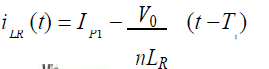
| At T2 the energy stored in LR is transferred to the output and the current becomes zero and the rectifier diodes DR1 and DR4 turn OFF. The resonant inductor current iLR(t) using initial condition iLR (0) = IP1 is given by |
 |
 |
 |
 |
C. Interval 3 (T2–T3) |
| Referring to Fig. 2, during this interval no power is transferred to the secondary. In this interval, the parasitic capacitances of the rectifier diodes resonate with LR. This resonance appears across the rectifier diodesDR1 andDR4 as illustrated in Fig. 2. For this interval, current in the resonant inductor remains zero (iLR = 0). |
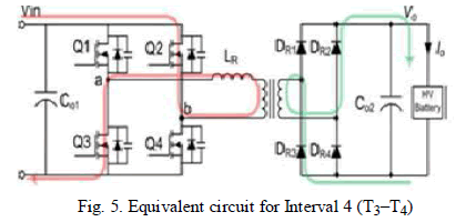
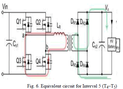
D. Interval 4 (T3–T4) Through Interval 6 (T5–T6) |
| Intervals 4 to 6 are the negative equivalent of Intervals 1 to 3 as shown in Figs 5 & 6. |
DESIGN CONSIDERATION |
| The proposed converter is operated is operated with 50% fixed duty cycle controlled switches (Q3 and Q4) can achieve both ZVS turn-on, and also the PWM controlled switches (Q1 and Q2) can achieve ZCS turnon. In addition, the secondary-side rectifier diodes can achieve ZCS, which reduces the reverse recovery losses due to the low di/dt. As an additional benefit, the voltage across the diodes is clamped to the output voltage, enabling the use of lower breakdown voltage diodes and eliminating the use of loss RCD voltage clamps, which are typically required in traditional CCM dc–dc converters with inductive output filters [11]–[13]. |
 |
 |
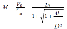
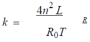
| The converter dc gain is given by equation (3), where n is the transformer turns ratio, D is the duty cycle, k is the normalized time constant of the converter, LR is the resonant inductor which also includes the leakage inductance of the transformer, R0 is the load resistance, and T is the switching period. |
 |
| The normalized time constant of the converter is given by |
 |
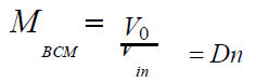
| The converter dc gain in BCM is given by |
 |
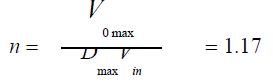
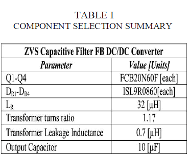
| The converter is designed to meet the specification shown in Table I. To meet the specifications, the t ransformer turns ratio n is designed for Vin = 400 V, Vomax = 450 V at maximum duty cycle of Dmax = 0.96. The transformer turns ratio is given by |
 |
| Using (3) to (5) the design curves shown in Fig. 11 are provided for gain versus duty cycle for various values of k in DCM. |
SIMULATION AND EXPERIMENTAL RESULTS |
| The performance of the converter designed in Section III was evaluated using MATLAB. Simulations circuit and results are shown. There is a close match between the theoretical prediction and simulation results. Experimental waveforms for DCM is shown. It is noted that the MOSFET Q3 turns ON with ZVS and turns OFF with ZCS and the current through the resonant inductor also has a very low di/dt. The voltage across the diode is clamped to the output voltage, and the di/dt through the diode is low enough to minimize the losses due to reverse recovery issues with ultrafast diodes. Waveforms of the ripple free output voltage and current. |
 |
| The efficiency of the proposed converter, particularly at light load conditions, is much higher than the benchmark converter. The benchmark converter has lower efficiency due to losses in the secondary side RCD clamp circuit. The performance of the proposed converter with Stealth diodes is very similar to that with silicon carbide (SiC) diodes. Therefore, this converter permits use of inexpensive hyperfast diodes, which are typically one quarter of the price of SiC diodes. |
 |
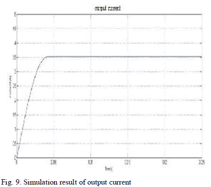 |
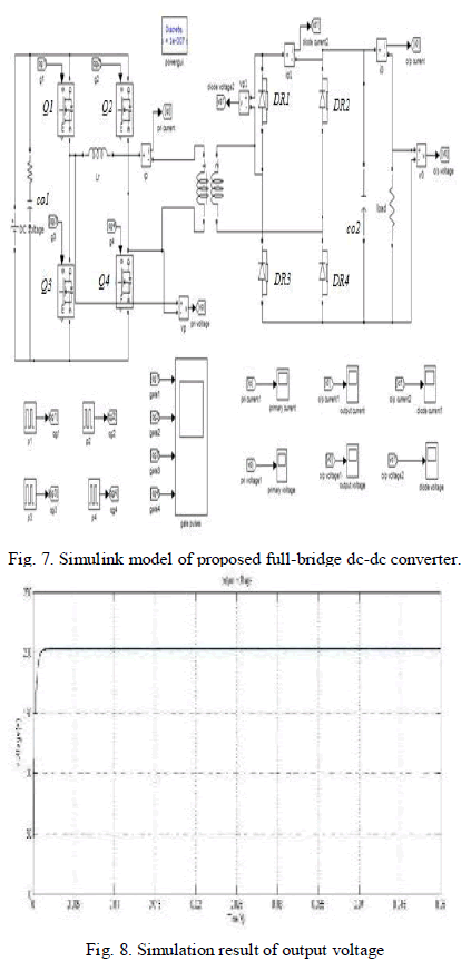
| Figure 7 shows the simulink model of the proposed resonant full bridge dc-dc converter and fig. 8 & 9 shows the output voltage and output current of the proposed dc-dc converter. |
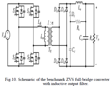 |
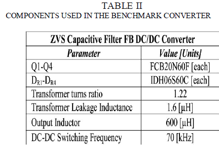
| Figure 10 shows the schematic diagram of benchmark ZVS full-bridge converter with inductive output filter. |
 |
| It has been shown that the converter achieves an overall peak efficiency with inexpensive hyperfast diodes. Finally, the converter performance in terms of cost, size, and efficiency is superior to its inductive output filter. The peak efficiency achieved is 92%. |
CONCLUSION |
| A ZVS full-bridge dc–dc converter with capacitive output filter has been presented for application in PHEV battery charging. The detailed operating intervals in DCM simulation results were presented. The proposed topology achieves soft switching for the full-bridge primary switches, naturally clamps the voltage across the output rectifier to the output voltage and the current through the rectifier diodes has a low di/dt, which minimize reverse recovery losses and increases the efficiency to 92%. |
References |
|