International Journal of Innovative Research in Science, Engineering and Technology
ISSN ONLINE(2319-8753)PRINT(2347-6710)
ISSN ONLINE(2319-8753)PRINT(2347-6710)
Satheyaraj. N1, Yamuna. K2
|
| Related article at Pubmed, Scholar Google |
Visit for more related articles at International Journal of Innovative Research in Science, Engineering and Technology
A Single Phase Single Stage Power Factor Corrected (SSPFC) AC/DC converter that operates with a single controller to obtain regulated dc output voltage is presented in this paper. The proposed converter integrates the operation of a boost power factor correction converter and a three-level DC/DC converter into one converter. . The existing converter has the problem of high component stress due to its three level structures. As the converter control is open loop a variable output voltage is not possible in the conventional system. The proposed system provides a closed loop control for variable output voltage. The SSPFC AC/DC converter can operate with lower peak voltage stresses across the switches and the DC bus capacitors as it is a three-level converter. This allows for greater flexibility in the design of the converter and ultimately improved performance. The output inductor of the converter can be designed to work in CCM mode over a wide range of load variation and input voltage. This results in a lower output inductor current ripple than that found in other two-level single-stage converter, which ultimately results in lower peak current stresses for the secondary components. . The operation of the converter is explained and its feasibility is confirmed with experimental result obtained from the simulation. The result shows that the new converter has better power factor for light load operation.
INTRODUCTION |
| The ac–dc power supplies with transformer isolation are typically implemented with some sort of input power factor correction (PFC) to comply with harmonic standards such as IEC 1000-3-2 [1]. There are three techniques to satisfy these standards. One of them is adding passive filter elements to the traditional passive diode rectifier/LC filter input combination; the resulting converter is very bulky and heavy due to the size of the low-frequency inductors and capacitors [2]. Another method is using an ac–dc boost converter in the front-end rectifying stage to perform active PFC for most applications. The ac–dc boost converter shapes the input line current as an almost sinusoidal shape with a harmonic content compliant with agency standards. Using active PFC, however, increases the cost and complexity of the overall two-stage converter because an additional switching converter must be implemented [2]. This has led to the emergence of single-stage powerfactor- corrected (SSPFC) converters. |
| There have been numerous publications about SSPFC converters, particularly for low-power ac–dc flyback and forward converters [1]–[11]. Research on the topic of higher power ac–dc single-stage full-bridge converters, however, has proved to be more challenging, and thus, there have been much fewer publications [12]– [14]. |
| There have been numerous publications about SSPFC converters, particularly for low-power ac–dc flyback and forward converters [1]–[11]. Research on the topic of higher power ac–dc single-stage full-bridge converters, however, has proved to be more challenging, and thus, there have been much fewer publications [12]– [14]. |
| The most common type of single-stage ac–dc full-bridge converter is based on some sort of voltage-fed single-stage pulse width modulation (PWM) converter [12]–[15]. Converters of this type have a large energystorage capacitor connected across their primary-side dc bus. They do not have the drawbacks of resonant and current-fed SSPFC converters. They operate with fixed switching frequency, and the bus capacitor prevents voltage overshoots and ringing from appearing across the dc bus and the 120-Hz ac component from appearing at the output. |
| Voltage-fed single-stage PWM full-bridge converters, however, have disadvantages that have limited their use. Most of these drawbacks are because 1) they are controlled by a single controller and the dc bus voltage is left unregulated [12]–[15]; and 2) they are implemented with two-level topologies that subject the converter components to high-voltage stresses [2], [12]– [15]. |
| With multilevel topologies, the dc bus voltage can be allowed to reach higher levels that are possible with a two-level topology as the converter components are exposed to half the dc bus voltage and, thus, have half the voltage stress. Freeing up the allowable limit of dc bus voltage allows the aforementioned limitations on output and input currents to be eased so that the converter can be made to operate with an output current that has less ripple and an input current that is less distorted than that of a two-level converter. |
| A three-level (TL) voltage-fed ac–dc singlestage PWM converter was proposed in [15] and is shown in Fig. 1. This topology does not have the drawbacks of previously proposed single-stage converters because of its TL structure. The variable output voltage is not possible due to its open loop control. The PWM method that was used to operate the converter is shown in Figure.2. |
 |
| A new TL ac–dc single-stage converter that can operate with standard phase-shift PWM is proposed in this letter. In this letter, the operation of the converter is explained, and its feasibility is confirmed with experimental results obtained from a prototype converter. Finally, the output voltage and power factor of the new converter is compared with that of the converter shown in Figure. 1. |
 |
II. PSM TECHNIQUE FOR TL SINGLE-STAGE CONVERTERS |
| The proposed converter, shown in Figure. 3, integrates an ac–dc boost PFC into a TL dc/dc converter. It is almost the same as the converter proposed in [15] and with a flying capacitor between two clamping diodes. The PFC is performed by using an auxiliary winding taken from the main transformer that acts like a switch that turns on and off in an appropriate manner. |
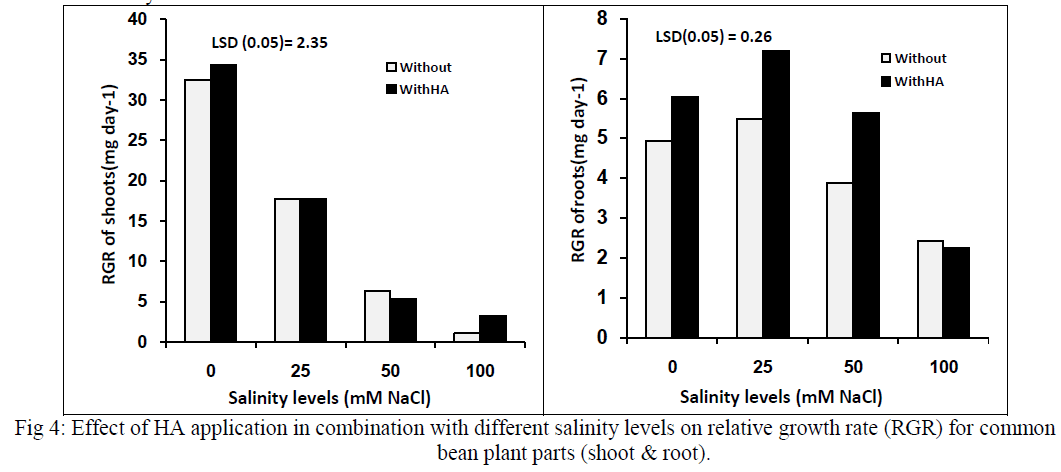
| The typical converter waveforms are shown in Fig.4 and equivalent circuit diagrams that show the converter modes of operation with Phase-Shift Modulation (PSM) are discussed in the following sections. The diode rectifier bridge output is replaced by a rectified sinusoidal source, and the thick lines represent the paths of current conduction. |
 |
| Mode 1 (t0 < t < t1) At time t0 switches S1 and S2 are ON, and energy from DC bus capacitor C1 is transferred to the output load. Since the auxiliary winding generates a voltage that is equal to the total DC-link capacitor voltage (sum of C1 and C2), the voltage across the input inductor is the rectified supply voltage, and thus, the input inductor current starts rising. The Figure.5 shows the operation of the new converter during Mode1. |
 |
| Mode 2(t1 < t < t2) At time t2, switches S1 is OFF and S2 remains ON. Capacitor Cs1 charges and capacitor Cs4 discharges through Cf until Cs4, the output capacitance of S4, clamps to zero. The energy stored in the input inductor during the previous mode starts to be transferred into the DC-link capacitors. This mode ends when S4 turns on with zero-voltage switching (ZVS). The Figure.6 shows the operation of the new converter during Mode1. |
| Mode 3 (t2 < t < t3) In Mode 3, S1 is OFF and S2 remains ON. The energy stored in the input inductor Lin during Mode 1is completely transferred into the DC-link capacitors. The amount of stored energy in the input inductor Lin depends upon the rectified supply voltage. This mode ends when the input inductor current reaches zero. Also, during this mode, the load inductor current freewheels in the secondary of the transformer. The Figure.7 shows the operation of the proposed converter during Mode 3. |
| Mode 4 (t3 < t < t4) At time t3 switch S1 is OFF, the primary current of the main transformer circulates through diode D1 and switch S2, and the load inductor current freewheels in the secondary of the transformer. The Figure.8 shows the operation of the new converter during Mode 4. |
 s s |
| Mode 5(t4 < t < t5) In this mode, S1 and S2 are OFF, and the current in the transformer primary charges capacitor C2 through the body diode of S3 and switch S4. This mode ends when switches S3 and S4 are switched on and a symmetrical period begins. In this mode, the load inductor current continues to transfer energy from the input to the output. The Figure.9. shows the operation of the proposed converter during Mode 5. |
 |
| Mode 6 (t5 < t < t6) At time t5, switche S3 is ON and S4 is OFF. The energy stored in the auxiliary inductors during the previous mode is completely transferred into the DClink capacitor. |
| Mode 7 (t6 < t < t7) At time t6, S4 is OFF and the primary current of the main transformer circulates through the diode D2 and S3. The output inductor current also freewheels in the secondary of the transformer during this mode. |
| Mode 8 (t7 < t < t8) At time t7, S3 andS4 is OFF and the primary current of the transformer charges the capacitor C1 through the body diodes of S1 and S2. Switches S1 and S2 are switched on at the end of this mode. |
III.SIMULATION CIRCUIT AND RESULTS FOR PROPOSED CONVERTER |
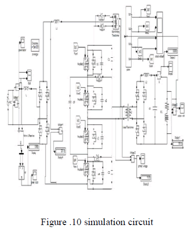
| The Figure.10. shows the simulation circuit for the closed loop control of the single phase SSPFC AC/DC converter.The proposed converter is similar to the converter presented in the chapter 3. The capacitor Cf is added between the clamping diode and the snubber capacitors are introduced to reduce the voltage stress across the MOSFET switches. The Power Factor Measurement circuit is similar to the circuit discussed in the previous chapter. The controller used to produce the gate pulse based on the PS-PWM technique. The PSPWM is an efficient technique used for voltage controlled multilevel inverter. PS-PWM is a carrier based PWM which uses multiple carrier with phase shifted with one another. Assume for an M-level inverter the PS-PWM technique requires (M-1) no of carrier and the carrier is shifted by (360/M-1). By considering this for three level output the PS-PWM requires 2 carrier signal each shifted by 180º. |
 |
| Here the triangular signal is used as a carrier signal hence after shifting it remains the same i.e single carrier is enough to produce three level output. The refrence signal is compared with the actual signal to produce error signal and fed to the PI controller. The PI controller output is compared with the carrier signal in the relational operator to produce gate pulse. |
IV.RESULT AND DISCUSSION |
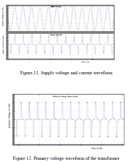
| The resulting waveforms for the proposed converter is discussed in this section. The supply voltage and current of the conventional converter is shown in the Figure.11. The input current is discontinuous and the input voltage is sinusoidal in nature. The current and the voltage are in phase with eachother. The magnitude of the voltage is 230VAC.the magnitude of the current is 0.6A AC. |
| Figure.12. shows simulation result of the primary voltage of the transformer. This is the three level wave form created by the multilevel inverter. The three level supply voltage is given to the transformer. The transformer ratio is 5:6 if the transformers input voltage is 85V means the output voltage of the transformer is 100V.The uncontrolled output in the primary voltage of the transformer in conventional system is eliminated in the proposed system. |
 |
| The Figure.13. shows the simulation waveform of the gate pulse produced using the PS-PWM techniques. In PS-PWM each switch conducts at different firing angle with same amplitude and pulse width. The three level voltage is obtained similar to the conventional converter. The voltage produced by the auxiliary winding is used to cancel the excess voltage in the capacitors(C1&C2). The load voltage is constant in the |
 |
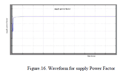
| The Figure.16 shows the simulation result of the supply power factor. The proposed converter has better power factor correction compared to the conventional converter for low power application. The proposed converter maintained a power factor of 0.99 for 20W RL load. conventional converter due its open loop control. The proposed converter implements the closed loop control using PS-PWM technique. Hence variable DC voltage (0- 100V DC) is possible in the conventional converter. Due to the closed loop control little distortion is occur at the output of the proposed converter. |
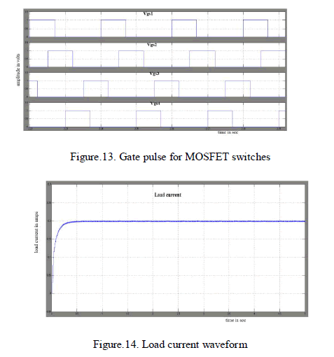 |
| The Figure.14. shows the load current waveform for RL load connected to the Single Phase SSPFC AC/DC Converter. The load current is continuos. The magnitude of the current waveform is approximately 0.2A. |
 |
 |
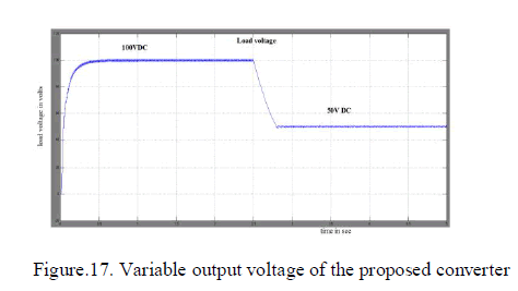 |
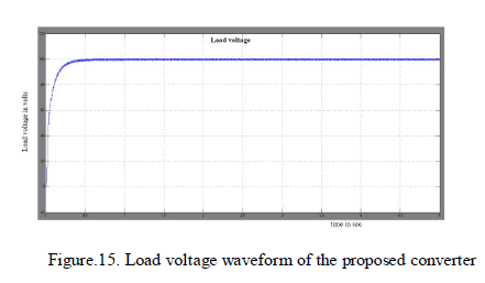
| The Figure.17 shows the variable load voltage of the proposed converter. The proposed SSPFC AC/DC Converter simulated is able to provide any desired voltage between (0-100 V DC) with improved power factor at the supply side. The Table.3 shows the simulaton parameters for the conventional and proposed system |
V. CONCLUSION |
| The purpose of the project was to develop closed loop control for the single-stage multilevel type full-bridge converter. A single phase SSPFC AC/DC converter that operates with a single controller to regulate the output voltage was presented. This converter has an auxiliary circuit that can cancel the capacitor voltage in which way the input inductor act as a boost inductor to have a single stage power factor correction. The outstanding features of the rectifier is that it can produce input currents that do not have dead band regions and an output current that can be continuous when the converter is operating from maximum load to at least half of the load. The converter can operate with lower peak voltage stresses across the switches and the DC bus capacitors as it is a three-level converter. This converter provides variable output voltage with improved power factor. This allows for greater flexibility in the design of the converter and ultimately improved performance. |
References |
|