Keywords
|
| Hybrid Electric Vehicles, Bidirectional DC-DC converter, Flyback Snubber, RCD Snubber, Active Clamp Snubber. |
INTRODUCTION
|
| Electric vehicles, Hybrid Electric Vehicles have been typically proposed to replace conventional vehicles in the near future. The inherent flexibility of Hybrid Electric Vehicles makes them suited for personal transportation and military applications. Hybrid Electric Vehicle combines the benefits of engine and electric motor to provide improved fuel economy. Engine provides most of the vehicle’s power and the additional power is provided by the motor when needed such as for accelerating and passing. The electric power for the motor is generated from regenerative braking and from the engine, so Hybrid Electric vehicle don’t have to be “plugged” into an electric outlet to recharge. |
| The bidirectional DC-DC converter is used for both stepping up and stepping down the voltage. Therefore, charging and discharging should be combined in one circuit topology. For the application where the output needs to be completely isolated from the input, isolated converters are employed. For high power applications, full bridge topology is used. |
| Fig.1 shows an overview of Hybrid Electric Vehicle. The major components are battery, engine, electric motor which can also work as generator and power electronic equipment. Hybrid Electric Vehicle combines the benefits of engine and electric motor to provide improved fuel economy. Engine provides most of the vehicle’s power and the additional power is provided by the motor, when needed, such as, for accelerating and passing. The electric power for the motor is generated from the regenerative braking or from the engine, so hybrid electric vehicles don’t have to be “plugged” into an electric outlet to recharge [4]. |
| When the vehicle is started, the engine warms up. If necessary, the electric motor acts as a generator, converting energy from the engine into electricity and stores in a battery. The engine powers the vehicle at cruising speeds and if needed, provides power to the battery for future use. During heavy acceleration, both engine and electric motor are used to propel the vehicle. While applying the brake, the kinetic energy of the motor is converted into electricity and this electric energy is stored in the battery. This operation is known as regenerative braking [4] [5]. |
| Batteries in a hybrid electric vehicle are usually required to backup power. Their voltage levels are typically much lower than dc bus voltage. The power electronic equipment used in the hybrid electric vehicle can perform both step-up and step-down operation. Here a bidirectional converter is used for both stepping up and stepping down the voltage and also for charging/discharging of the batteries. |
CIRCUIT DESCRIPTION
|
| The bidirectional DC-DC converter is used for both stepping up and stepping down the voltage. Therefore, charging and discharging can be combined into one circuit topology. For the application where the output needs to be completely isolated from the input, isolated converters are employed. For high power applications, full bridge topology is used [7]. |
| In Fig.2, the left hand side is a low voltage side and right hand side is a high voltage side. Low voltage side consists of battery and current fed full bridge and high voltage side consist of voltage fed full bridge. Low voltage side and high voltage side is separated by an isolation transformer with turns ratio, 1:n. Inductor, Lm acts as boost inductor when power flows from the low voltage side to high voltage side, which is described by boost mode of operation. On the other hand, inductor, Lm performs output filtering, when power flows from high voltage to low voltage side, which is described by buck operation. But in the main circuit, there can occur over voltage and over current stress across the MOSFET switches which can be reduced by the snubber circuits [7]. |
OPERATION OF THE PROPOSED CONVERTER
|
| A. STEP-UP CONVERSION |
| In boost mode, switchesM1–M4are operated like a boost converter, where switch pairs (M1, M2) and (M3, M4) are turned ON to store energy in Lm. At the high-voltage side, the body diodes of switches M5–M8 will conduct to transfer |
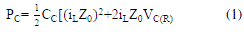
| power to VHV. When switch pair (M1, M2) or (M3, M4) is switched to (M1, M4) or (M2, M3), the current difference iC (= iL− ip) will charge capacitor CC , and then, raise ipup to iL. The clamp branch is mainly used to limit the transient voltage imposed on the current-fed side switches. Moreover, the flyback converter can be controlled to charge the high-voltage-side capacitor to avoid over current. The clamp branch and the flyback snubber are activated during both start-up and regular boost operation modes. A non-phase-shift PWM is used to control the circuit to achieve smooth transition from start-up to regular boost operation mode. Referring to Fig. 3.1, the average power PC transferred to CC can be determined as follows: |
 |
 |
 |
| where, VC (R) stands for a regulated VC voltage, which is close to (VHV(NP /NS)), fs is the switching frequency, and Lm>>Leq. Power PC will be transferred to the high-side voltage source through the flyback snubber, and the snubber will regulate clamping capacitor voltage VC toVC(R) within one switching cycle Ts. Note that the flyback snubber does not operate over the interval of inductance current ip increasing toward iL. The processed power PC by the flyback snubber is typically around5% of the full-load power for low-voltage applications. With the flyback snubber, the energy absorbed in CC will not flow through switches M1–M4, which can reduce their current stress dramatically when Leq is significant. Theoretically, it can reduce the current stress from 2iLtoiL. The peak voltage VC (P)of VC will impose on M1–M4 and it can be determined as follows: |
 |
| where, iL(M) is the maximum inductor current of iL, which is related to the maximum load condition. Additionally, for reducing conduction loss, the high-side switchesM5–M8are operated with synchronous switching. Reliable operation and high efficiency of the proposed converter are verified on a prototype designed for alternative energy applications. |
| First of all switches M1-M4 are turned on, so the primary side of the transformer is short circuited and therefore VAB=0. Inductor, L is charged by the battery. At t1, M1& M4 remain conducting, so VAB is present. Clamping diode, Dc continues to conduct until the current difference drops top zero at t2. Moreover D5 and D8 are conducting to transfer the power. During this interval (iL-iP) flows into clamping capacitor. So clamp capacitor voltage, VC is rising at the interval t1-t2 and ip= iL condition is reached. During t2 -t3, Dc stops conduction and flyback snubber starts to operate. Cc is discharging and the flyback switch is turned on and the energy is stored in flyback snubber as flux. In the interval t3-t4 energy stored in the inductor is transferred to high voltage side. Over this interval, flyback snubber will operate independently to regulate VC to VC(R). Energy stored in the transformer of the flyback snubber is transferred to the output when flyback switch turns off. At t4,Vc has been regulated to VC(R) and the snubber remains idle. Over this interval the main power stage is still transferring power from low voltage to high voltage side. It stops at t5 and completes a half switching cycle operation. |
| B.STEP-DOWN CONVERSION |
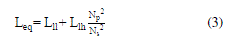
| In the analysis, leakage inductance of the transformer at the low-voltage side is reflected to the high-voltage side, as shown in Fig. 2, in which equivalent inductance, L* eq equals the summation of ll and lh p s . This circuit is known as a phase-shift full-bridge converter. In the step-down conversion, switches M5–M8 are operated like a buck converter, in which switch pairs (M5 , M8 ) and (M6 , M7 ) are alternately turned ON to transfer power from VHV to VLV. |
| SwitchesM1–M4are operated with synchronous switching to reduce conduction loss. For alleviating leakage inductance effect on voltage spike, switchesM5–M8are operated with phase-shift manner. Although, there is no need to absorb the current difference between iLand ip, capacitor, CC can help to clamp the voltage ringing due to Leq and parasitic capacitance of M1–M4.An isolated bidirectional full bridge DC-DC converter with low-side voltage of 48 V, high side voltage of 360 V, and power rating of 1.5 kW has been designed and implemented. The proposed topology and control is particularly relevant to multiple voltage electrical systems in hybrid electric vehicles and renewable energy generation systems. |
| During the time period t0-t1, switches M5 and M8 are on, while switches M6 and M7 are in the off state. High side voltage is immediately exerted on the transformer and the whole voltage is exerted on the transformer causing current to rise. With transformer current, is increasing linearly towards the load current at t1, switches, M1 and M4 are conducting to transfer the power and the voltage across the transformer terminals on the current fed side changes immediately to reflect the voltage from the voltage fed side. |
| At t1, switch M8 remain conducting, while switch M5 is turned off. Diode, D6 starts to conduct the freewheeling leakage current. Transformer current reaches the load current level at t1 and starts to decrease during the interval t1-t2 and voltage VAB starts to decrease. The clamping diode, Dc starts to conduct during this interval. |
| At t2, with diode, D6 conducting, switch, M6 can be turned on under ZVS. At t3, switch M6 remains conducting, while switch, M8 is turned off. Diode, D7 then starts to conduct the freewheeling leakage current. |
| At t4, with the diode, D7 conducting, switch M7 can be turned on under ZVS. Over this interval, the active switches change to the other pair of diagonal switches and the voltage on the transformer reverse its polarity to balance the flux and to alleviate the transient voltage problem. It stops at t5 and completes a half switching cycle operation. |
| A closed loop speed control technique of the proposed battery fed electric vehicle is designed and implemented using PI controller. |
SIMULATIONS AND RESULTS
|
| The simulation of the proposed paper is carried out using MATLAB software. The open and closed loop simulation of buck mode and boost mode is done separately. For open loop simulation, PWM pulses are given as the gating signal. For closed loop simulation, a voltage and current feedback circuit is considered. The isolated bidirectional DC-DC full bridge converter with and without flyback snubber is simulated. The battery fed drive for electric vehicles using isolated bidirectional DC-DC converter with a flyback snubber is also simulated. The simulations are performed with following parameters and the design procedure is explained earlier. |
| A. SIMULATION RESULTS OF BOOST OPERATION |
| We obtain an output voltage of 381.2V for open loop bidirectional full bridge DC-DC converter without flyback snubber. |
| We obtain a speed of 58.1rad/sec for of bidirectional full bridge DC-DC converter with flyback snubber- Boost open loop operation. |
| B. SIMULATION RESULTS OF BUCK OPERATION |
| We obtain an output voltage of 42.86V for open loop bidirectional full bridge DC-DC converter without flyback snubber- Buck operation |
| The simulation results of open loop and closed loop control of isolated bidirectional DC-DC converter with and without flyback snubber for various loads are done. DC motor as a load is used for the simulation in hybrid vehicle application. |
CONCLUSION
|
| Bidirectional dc-dc converters (BDC) have recently received a lot of attention due to the increasing need of systems with the capability of bidirectional energy transfer between two dc buses. Apart from traditional application in dc motor drives, new applications of BDC include energy storage in renewable energy systems, fuel cell energy systems, hybrid electric vehicles (HEV) and uninterruptible power supplies (UPS). |
| An isolated bidirectional dc-dc converter with a flyback snubber is presented. The flyback snubber can alleviate the voltage spike caused by the current difference between the current fed inductor and leakage inductance of the isolation transformer, and can reduce the current flowing through the active switches. Since the current does not circulate through the full bridge switches, their current stress can be reduced dramatically. The work demonstrates the performance of a hybrid electric vehicle system and it shows satisfactory performance at different driving condition. The proposed control technique with PI controller find suitable for this electric drive. |
Tables at a glance
|
 |
| Table 1 |
|
| |
Figures at a glance
|
 |
 |
 |
 |
 |
| Figure 1 |
Figure 2 |
Figure 3 |
Figure 4 |
Figure 5 |
 |
 |
 |
 |
 |
| Figure 6 |
Figure 7 |
Figure 8 |
Figure 9 |
Figure 10 |
 |
 |
 |
 |
 |
| Figure 11 |
Figure 12 |
Figure 13 |
Figure 14 |
Figure 15 |
 |
 |
 |
| Figure 16 |
Figure 17 |
Figure 18 |
|
| |
References
|
- C.Zhao, S. D. ound, and J.W.Kolar, “An isolated three-port bidirectional DC-D converter with decoupled power flow management”, IEEE TransactionsPower Electronics, vol. 23, no. 5, pp. 2443–2453, Sep. 2008.
- Gang Ma, W. Qu, Gang Yu, Y. iu, .iang, and W. i, “A zero-voltage-switching bidirectional dc–dc converter with state analysis and soft-switching-oriented design consideration”, IEEE TransactionsPower Electronics, vol. 56, no. 6, pp. 2174–2184, June 2009.
- H. Xiao and S. Xie, “A S bidirectional dc-dc converter with phased shift plus WM control scheme”, IEEE Transactions Power Electronics, vol. 23, no. 2, pp. 813–823, Mar. 2008.
- P.Pany, R.K. Singh, R.K. Tripathi , “Bidirectional D -D converter fed drive for electric vehicle system”, International Journal of Engineering, Science and Technology, Vol. 3, No. 3, pp. 101-110,May 2011
- O. García, .A. Flores, J.A. Oliver, J.A obos, and J. de la ena, ‘Bi-directional dc-dc converter for hybrid vehicles”, IEEE Transactions ower Electronics, vol. 7, no. 3, pp. 1881-1886, March 2005.
- H.Bai and .Mi, “Eliminate reactive power and increase system efficiency of isolated bidirectional dual-active-bridge DC-DC converters using novel dual-phase-shift control”, IEEE Transactions Power Electronics, vol. 23, no. 6, pp. 2905–2914, Dec. 2008.
- T. Wu,, Y. hu hen, J. Yang, and . Kuo, “Isolated Bidirectional Full-Bridge DC–D onverter With a FlybackSnubber”, IEEE Transactions Power Electronics,pp 1915- 1922, July, 2010.
- T F Wu, Y D hang, H hang, and J G Yang, “Soft-switching boost converter with a flybacksnubber for high power applications”, IEEE TransactionsPower Electronics, vol. 27, no. 3, pp. 1108-1119, March 2012.
- B. Bai, .Mi, and S. Gargies, “The short-time-scale transient processes in high-voltage and high-power isolated bidirectional DC-D converters”, IEEE Transactions Power Electronics, vol. 23, no. 6, pp. 2648–2656, Nov. 2008.
|