Keywords
|
| Multilevel inverter, Total Harmonic Distortion, Fundamental Frequency Modulation technique, Sinusoidal Pulse Width Modulation Technique. |
INTRODUCTION
|
| Multi Level Inverter (MLI) plays an important role in the area of power electronics and it is widely used in industrial and renewable energy applications. It is not only achieves high power ratings, but also enables the use of renewable energy sources. Renewable energy sources such as photovoltaic, wind, and fuel cells can be easily interfaced to a multilevel converter system for high power application. The concept of multilevel converters has been introduced since 1975. The term multilevel began with the three level converter. Subsequently, several multilevel converter topologies have been developed .It is classified into a) Diode clamped multilevel inverter b) Flying capacitor multilevel inverter c) Cascaded H-bridge multi level inverter. Among these topologies, cascaded MLI is preferred as it requires minimum number of components to implement higher number of levels. This paper focuses on a seven level cascaded H-bridge inverter with reduced number of dc sources which overcomes the disadvantages of the conventional multi level inverter. The proposed inverter has reduced dc sources and power electronic switches. Moreover, this paper proposes a new hybrid modulation technique employing single and double carrier signals in order to obtain a reduced THD. The performance of the inverter is studied in terms of spectral quality of the output and it is analyzed for various modulation indices and the results are discussed. MATLAB/SIMULNK software is employed to carry out the simulation of the proposed inverter structure. |
LITERATURE REVIEW
|
| Jinn-Chang Wu and Chia-Wei Chou (2014) have proposed a seven-level inverter with only six power electronic switches and only one power electronic switch is switched at high frequency which is suitable for solar power generation system. The proposed inverter structure generates a sinusoidal output current that is in phase with the utility voltage and is fed into the utility. N.A.Rahim,K.Chaniago,and J.Selvaraj(2011) have proposed a single phase seven level inverter for grid connected PV system with a novel PWM control scheme. This technique employs three reference signal and single triangular carrier signal to generate PWM signals for the switches. J.Pereda and J.Dixon(2011) have proposed Asymmetrical CHB (ACHB) inverter uses one dc supplies with different voltages, increasing the power quality (number of levels).ACHB improves the efficiency. It operate at the fundamental frequency, reducing the switching losses. Moreover, the THD is highly reduced, therefore output filters can be eliminated. |
PROPOSED SEVEN LEVEL INVERTER
|
| Fig 1 shows a seven level inverter together with dc-dc power converter. The proposed system consist of new seven level inverter and DC/DC power converter. The DC/DC power converter consists of DC/DC boost converter and current fed forward converter. DC/DC power converter is used to convert the dc voltage into two independent voltage sources. The new seven-level inverter is composed of capacitor selection circuit and full bridge converter. The capacitor selection circuit and full bridge converter converts two independent three level dc voltage and the full bridge converter converts the three-level dc voltage into seven level ac voltage. |
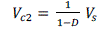
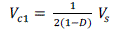
| DC-DC power converter is composed of boost converter and current fed forward converter with turns-ratio of 2:1.Fig 2 shows the operation of DC-DC power converter. When switch SD1 is turned ON, boost converter charges the capacitor C2 of the new seven level inverter. When switch SD1 is turned OFF and SD2 is turned ON , the current fed forward converter charges the C1 of the new seven level inverter. The voltage across the C2 is |
 eq.(1) eq.(1) |
| Vs is supply voltage and D is duty ratio of SD1.The voltage across the C1 is |
 eq.(2) eq.(2) |
| Fig 3 shows operating circuit of new seven level inverter (Zero, Vdc/3, 2Vdc/3, Vdc, -2Vdc/3, -Vdc/3, -Vdc). The voltage across C1 and C2 are constant and equal to Vdc/3 and 2Vdc/3.ie.the input voltage is 70, the voltage of the capacitor C1 is 70V and voltage of the capacitor C2 is 140V.All switches are operated in fundamental frequency. The circuit operation is explained as follows. The circuit operation of seven level inverter classified as 8 modes. Positive half cycle have 4 modes and negative half cycle have 4 modes. |
| Mode 1: In this mode, switches S1 and S4 conducts, switches SS1 and SS2 are turned off. The capacitor C1 discharges through the diode D1.so the output voltage of the inverter is Vdc/3. |
| Mode 2: In this mode, switches SS2, S1 and S4 conducts, switch SS1 is turned off. The capacitor C2 discharges through the diode D2.so the output voltage of the inverter is 2Vdc/3. |
| Mode 3: In this mode, switches SS1, SS2, S1 and S4 conducts, both the capacitors C1 and C2 discharges through the diode D1 and D2 so the output voltage of the inverter is Vdc. |
| Mode 4: In this mode, switches S2 and S4 conducts, other switches are turned off, so the output voltage of the inverter is zero. |
| Mode 5: In this mode, switches S2 and S3 conducts, switches SS1 and SS2 are turned off. The capacitor C1 discharges through the diode D1, so the output voltage of the inverter is -Vdc/3. |
| Mode 6: In this mode, switches SS2, S2 and S3 conducts, switch SS1 is turned off. The capacitor C2 discharges through the diode D2.so the output voltage of the inverter is -2Vdc/3. |
| Mode 7: In this mode, switches SS1, SS2, S2 and S3 conducts, both the capacitors C1 and C2 discharges through the diode D1 and D2.so the output voltage of the inverter is -Vdc. |
| Mode 8: In this mode, switches S2 and S4 conducts, other switches are turned off. So the output voltage of the inverter is zero. |
PWM TECHNIQUES
|
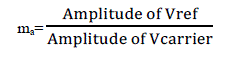
| In MLI, seven-level output voltage is obtained by different combination of conduction state of six switches. The gating pulse for these switches are given by using hybrid modulation which is the combination of fundamental frequency modulation (FPWM) and sinusoidal PWM. In the sinusoidal PWM, two methods are employed namely: |
| • Single Carrier Modulation of MLI |
| • Dual Carrier Modulation of MLI |
 eq.(3) eq.(3) |
| Frequency modulation ratio (mf) can be expressed as, |
 eq.(4) eq.(4) |
| where, fs is PWM frequency and f1 is fundamental frequency. mf should be an odd integer, otherwise DC component may exist and even harmonics will be present at the output voltage. mf should be a multiple of three for three-phase inverter. Fig 4.shows a carrier and reference waveform for single carrier modulation technique. Fig 5. shows the carrier and reference waveform for dual carrier modulation technique. |
| By comparing different PWM Techniques based on THD values, dual carrier PWM technique has reduced THD and produces better quality output. |
SIMULATION RESULTS
|
| The single-phase seven-level inverter topology for the proposed modulation strategies namely single carrier and dual carrier PWM was simulated in MATLAB and is shown below. The simulation was carried out with an input voltage of 70V and switching frequency is 15150Hz.The other simulation parameters are shown in Table 2. |
| The simulink model is shown in Fig.6.The output voltage and THD have been compared so as find out the best suitable strategy for seven level inverter. Figs.7 & 8 show the output load voltage waveforms for single carrier PWM and dual carrier PWM. |
| Figs 9 & 10 show the FFT spectrum of the output voltage of the seven-level inverter for single and dual carrier PWM techniques. Fig.11 &12 shows the THD Vs ma and THD Vs switching frequency for dual carrier PWM method. |
| The THD values for the seven level inverter with dual carrier PWM was around 24.94% when the modulation index was equal to 0.9. The Modulation index decreased to 0.8 as the inverter output voltage THD was equal to 26.72%.i.e when the modulation index increases it reduces the THD values. |
| The THD values for the seven level inverter with dual carrier PWM was around 24.94% when the switching frequency was equal to 15150Hz, as shown in Fig12.The switching frequency decreased to 3150Hz as the inverter output voltage THD was equal to 25.01% i.e when the switching frequency increases it reduces the THD values. From the simulation results, it is inferred that the dual carrier PWM technique provides a reduced THD compared to single carrier one. Therefore, dual carrier PWM method is found to be suitable for the proposed MLI for PV applications. |
CONCLUSION
|
| This paper has presented a single-phase seven level inverter with reduced number of switches. A single and dual carrier modulation method have been proposed. It is found that dual carrier modulation gives a reduced THD compared to single carrier modulation and it gives a better quality output. Therefore, PV is recommended for the proposed inverter with reduced number of switches. Hence, seven-level inverter with reduced component along with dual carrier PWM technique will enhance the quality of the output and provides a better efficiency for suited for PV applications. |
Tables at a glance
|
 |
|
| Table 1 |
Table 2 |
|
| |
Figures at a glance
|
 |
 |
 |
 |
 |
| Figure 1 |
Figure 2 |
Figure 3 |
Figure 4 |
Figure 5 |
 |
 |
 |
 |
 |
| Figure 6 |
Figure 7 |
Figure 8 |
Figure 9 |
Figure 10 |
 |
 |
| Figure 11 |
Figure 12 |
|
| |
References
|
- Jinn-Chang Wu and Chia-Wei Chou, “A Solar Power Generation System With a Seven-Level Inverter”, IEEE Trans.Power Electron.,Vol 29,No.7,pp.3454-3462,July 2014.
- N. A. Rahim, K. Chaniago, and J. Selvaraj, “Single-phase seven-level grid-connected inverter for photovoltaic system”, IEEE Trans. Ind. Electr., Vol. 58, no. 6, pp. 2435–2443, June. 2011.
- J. Pereda and J. Dixon, “High-frequency link: A solution for using only one DC source in asymmetric cascaded multilevel inverters”, IEEE Trans.Ind. Electron., Vol. 58, no. 9, pp. 3884–3892, September. 2011.
- T. Porselvi and RanganathMuthu, “seven-level three phase cascaded h-bridge inverter with a single dc source”, ARPN Journal of Engineering and Applied Sciences, Vol. 7, no. 12, December 2012 ISSN 1819-6608
- T. Singaravelu, M.Balasubramani ,J.Gowrishankar, “Design and Implementation of Seven Level Cascaded H-Bridge Inverter Using Low frequency transformer with Single DC Source”,Vol 5 No 3 Jun-Jul 2013, ISSN : 0975-4024.
- E. Pouresmaeil, D. Montesinos-Miracle, and O. Gomis-Bellmunt, “Control scheme of three-level NPC inverter for integration of renewable energy resources into AC grid,” IEEE Syst. J., Vol. 6, no. 2, pp. 242–253, Jun2012.
- Gobinath.K, Mahendran.S, Gnanambal.I,“New Cascaded H-Bridge Multilevel Inverter With Improved Efficiency” ,International Journal of Advanced Research in Electrical, Electronics and Instrumentation Engineering Vol. 2, Issue 4, April 2013.
- Jacob James Nedumgatt, Vijayakumar D, A. Kirubakaran, Umashankar S, “A Multilevel Inverter with Reduced Number of Switches”, IEEE Students’ Conference on Electrical, Electronics and Computer Science,2012.
- T.V.V.S.Lakshmi, Noby George, NandithaSundaresan, Harisankar.M.A, Umashankar.S, “Cascaded seven level inverter with reduced number of switches using level shifting PWM technique”, International Conference on Power, Energy and Control (ICPECT) 2013.
- M.F.Kangarlu,E.Babaei,S,Laali,“Symmetric multilevel inverters with reduced components based on non isolated dc sources”, IET Power Electron., Vol.5,pp. 571-581,2012,.
|