Keywords
|
| Coulomb blockade, Single electron tunnelling, Threshold logic gate, Tunnel junction. |
INTRODUCTION
|
| Single electronics have attracted much attention because of their very low power consumption and ultra small size [1]. The ever-decreasing size and the corresponding increase in the density of transistors facilitated improvements in semiconductor based designs. The MOS technology will presumably be continued for some more years by the wellknown scaling of structure geometry [2]. There have been reports suggesting that the MOS transistor cannot shrunk beyond certain limits [3]. Single Electronics is a possible successor technology with greater scaling potential. The Single Electron Tunneling (SET) technology is the most promising future technology to meet the required increase in density, performance and decrease in power dissipation [4, 5]. The main device of the SET circuits is the tunnel junction through which individual electrons can move in a controlled manner [5]. The operation of the tunnel junction is based on the Coulomb blockade [6]; the tunneling of an electron into an ultra small conductive island is inhibited by the charging energy. There are many reports on SET transistors using metals, GaAs, and Si [7]. Single-electron memories using metals and Si have also been widely investigated [7]. Any function can be computed using a network of conventional Boolean gates such as AND, OR, NAND and NOR logic gates. However, there are alternative logic design styles, such as threshold gate based logic, that may be more suitable for novel technologies such as single electron tunnelling technology. Threshold gates are fundamentally more powerful than the conventional Boolean gates. Moreover a number of theoretical investigations suggest that threshold logic may be a promising design approach. |
| In this paper, we first briefly discuss the basic physics of single electron devices. Some single electron device based threshold logic gates like OR, AND and Buffer/NOT are described. A control unit for a chemical process is described, designed and implemented with Single electron device based threshold logic gates. Analysis of the proposed control unit and results are also discussed. |
THE BASIC PHYSICS
|
| The basic component of single electronics is the tunnel junction. A tunnel junction can be considered as two conductors separated by a thin layer of insulating material as shown in Fig. 1. A tunnel junction can be thought of as a leaky capacitor [8] which is characterised by a capacitance Cj and a resistance Rj, each of which depends on the physical size of the tunnel junction and the thickness of the insulator. The transport of electron through a tunnel junction is called tunneling. |
| Electrons are considered to tunnel through a tunnel junction one after another [8, 9]. Even only one electron tunnelling may produce a potential e/C across the tunnel junction (where C is total capacitance and e = 1.602 x 10⁻¹⁹ C). The threshold voltage which is the voltage needed across the tunnel junction for an electron to tunnel through the junction is called the critical voltage (Vc) and is given by [8]: |
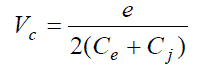 (1) (1) |
| In (1), Cj is the junction capacitance and Ce is the equivalent capacitance for remainder circuit as viewed from the tunnel junction’s perspective. Tunnel event will occur across the tunnel junction if and only if the voltage Vj across the tunnel junction is greater than or equal to Vc i.e Vc, otherwise the tunnel event cannot occur. The circuit will be in stable state if Vc. |
| A Threshold Logic Gate |
| Threshold logic gates (TLG) are devices which can compute any linearly separable Boolean functions given by [8]. |
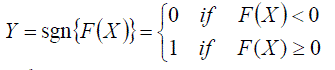 (2) (2) |
| and |
 (3) (3) |
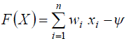
| Where is a threshold value, xi is the ith input and wi is the corresponding integer weight. If the weighted sum of inputs n i wi xi 1 is greater than or equal to the gate produces logic 1 at the output; otherwise output will be logic 0. |
| The TLG gate symbol and structure of n input TLG are depicted in Figs 2(a) and 2(b). The input voltages Vp weighted by their input capacitances Cp are added to Vj and the input voltages Vn weighted by their input capacitances Cn are subtracted from Vj. The critical voltage Vc of the tunnel junction which can be adjusted by the bias voltage Vb weighted by Cb acts as the threshold value. The function F(X) for the circuit is given by |
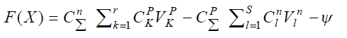 (4) (4) |
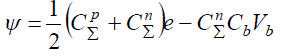 (5) (5) |
| The generic threshold gate describe here can be used to implement any logic function. To prevent loading effect as well as to maintain correct voltage levels, SET buffer/inverting are connected at the output of the TLG (10). The circuit of such buffer/inverter is shown in Fig. 3. |
DESIGN OF THE PROCESS CONTROLLER
|
| A block diagram of a process controller which is taken from Ref. 10 is shown in figure 4 for convenience of discussion. Temperature and pressure are the input variables. The output variables are the signals to the heater, valve and alarm. |
| The control is exercised by switching on or off a heater and by opening or closing a valve. The control rules are given below [10]: |
| 1. If temperature and pressure are in the normal range, switch off the heater and close the valve. |
| 2. If the temperature is normal, switch off the heater. Open the valve if the pressure is above normal and close it if it is below normal. |
| 3. If the pressure is normal, close the valve. Turn on the heater if the temperature is below normal and turn it off if the temperature is above normal. |
| 4. If the pressure is above normal and the temperature is below normal open the valve and turn off the heater. |
| 5. If the temperature is above normal and the pressure is below normal, turn off the heater and close the valve. |
| 6. If both temperature and pressure are above or below normal, ring an alarm and shut down the plant. |
| The temperature and pressure variables are coded as shown in table 1 and the output variables are coded as shown in table 2. |
| The truth table for the controller to be designed is shown in Table 3. |
| The logic expressions for implementation of the control unit are H B.C , V C and R B.D , The design is done following conventional digital system design scheme which can be found in Ref. 10 and hence not detailed here. Here, we are interested in the single-electron threshold logic based implementation of the controller. The logic circuit of the process controller is shown in Fig 5. |
| The threshold equations for 2-input AND and 2-input OR gates can be written as |
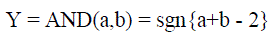 (6) (6) |
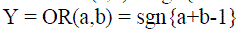 (7) (7) |
| There may be variations in circuit parameters in any circuit. To maximize robustness for such variations in parameter values, the threshold value =I (i being an integer) is replaced by the average of the interval ( i.e =i-1/2) [8] and (6) and (7) are written as |
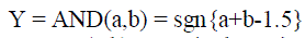 (8) (8) |
 (9) (9) |
| Both 2-input AND and 2-input OR gates have the same LTG structure but they will have different circuit parameter values. The structure of 2-input AND/OR gate is shown below. |
| When a buffer is connected, we need to reverse the positively and negatively weighted inputs in the logic function accordingly. The structure of buffered 2-input AND/OR gate is shown in Fig. 6. |
| The threshold equation of the buffered gates can be written as |
| Y = AND(a,b) = sgn{-a-b+1.5} (10) |
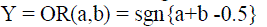
| Y = OR(a,b) = sgn{-a-b+0.5} (11) |
| Assuming logic ’0’=0 V, logic’1’=16mV, Rj=105 ohm and Cj=0.1aF, the values of the circuit parameter are designed for 2-input AND gate from equations (4), (5) and (10) and for the OR gate from equations (4), (5) and (11), respectively. The values are given in Table II. For the buffer/inverter, circuit parameters values are taken from Ref. 7. |
RESULT AND DISCUSSION
|
| The proposed process control unit is verified by simulation using SIMON [11]. The complete circuit of Single Electron TLG based Process control circuit is given in Fig. 7. |
| Fig. 8 shows the results of the simulation. In the simulation, A, B, C and D are the input variables; H, V and R the output variables. The results obtained from the simulation are found to be satisfactory |
CONCLUSION
|
| The design and simulation of control unit of a process controller using Single Electron Threshold Logic Gate is presented. The complete circuit to implement the control unit has been designed and verified by simulation with SIMON. The performance of the control unit is found to be satisfactory thereby establishing the feasibility of future much faster VLSI/ULSI circuits using SET-based TLGs. |
Tables at a glance
|
 |
|
|
|
| Table 1 |
Table 2 |
Table 3 |
Table 4 |
|
| |
Figures at a glance
|
 |
 |
 |
 |
 |
| Figure 1 |
Figure 2 |
Figure 3 |
Figure 4 |
Figure 5a |
 |
 |
 |
 |
| Figure 5b |
Figure 6 |
Figure 7 |
Figure 8 |
|
| |
References
|
- K. Likharev,”Single-Electron Devices and Their Application,” Proc. IEEE, vol.87, no. 4,pp. 606-632,1999.
- W. R Fahrner,”Nanotechnology and nanoelectronics-Materials, Devices, Measurement Techniques,” Springer Indian Reprint, 2006.
- Y.Tau, D.A.Buchanan, W.Chen, D.Frank, K.Ismail, S.Lo, G.Sai-Halasz, R.Viswanathan, H.Wann, S.Wind, and H.Wong, “CMOS Scaling intothe Nanometer Regime,” Proceeding of the IEEE, vol.85, pp. 486–504, 1997.
- “Technology Roadmap for Nano-electronics,” http://www.cordis.lu/esprit
- S. Cotofana, C. Lageweg, and S. Vassilidis, “Addition Related Arithmetic Operations via Controlled Transport of Charge,” IEEE Trans. OnComputers, vol. 54, no.3, 2005.
- D. V. Averin, and K. Likharev, ”Coulomb blockade of tunneling, and coherent oscillations in small tunnel junctions,” J. Using equations 5and 6, tLow Temp. Phys. 62, 345-372,1986.
- C. Lageweg, S. Cotofana, and S. Vassilidis, “Single Electron Encoded Latches and Flip-Flops,” IEEE Trans. On Nanotechnology, vol. 3, no.22004.
- JialinMi; Chunhong Chen; “Finite state machine implementation with single- electron tunneling technology” IEEE Computer Society annualsymposium on Emerging VLSI Technologies and Architectures, 2006.
- C.Lageweg and S.Cotofana and S.Vassiliadis,”Achieving Fanout Capabilities in Single Electron Encoded Logic Networks,” 6th InternationalConference on Solid-State and IC Technology (ICSICT), October 2001.
- V. Rajaraman and T. Radhakrishnan, “Digital Logic and Computer Organization,” Prentice-Hall of India, New Delhi, pp.78-81, 2006.
- ChristophWasshuber, “Single-Electronics – How It Works. How It’s Used. How It’s Simulated,” IEEE Proceedings of the International.
- Symposium on Quality Electronic Design (ISQED.02), pp. 502-507, 2002.
> |