International Journal of Advanced Research in Electrical, Electronics and Instrumentation Engineering
ISSN ONLINE(2278-8875) PRINT (2320-3765)
ISSN ONLINE(2278-8875) PRINT (2320-3765)
Kavya Jyothi.B1, Dr. K.B.Shivakumar 2, Dr.M.Z.Kurian3, Prof. Imran Rasheed4
|
| Related article at Pubmed, Scholar Google |
Visit for more related articles at International Journal of Advanced Research in Electrical, Electronics and Instrumentation Engineering
Area occupied by an FIR(Finite Impulse Response) filter increases as the order of the filter increase. This is due to the increase in the number of multipliers in the parallely implemented MAC (Multiply and Accumulate) structure. This paper presents an efficient design for the implementation of BP FIR filter on FPGA (Field Programmable Gate Array) using DA (Distributed Arithmetic) architecture. DA replaces multipliers by LUTs( Look Up Tables), adders and shift registers. Hence optimal resource utilization is possible, as number of fully utilized LUT flip flop pair increases. In addition DA technique adopts pipelined processing of data. Hence throughput can be increased by increasing the number of pipelined stages. A verilog code is developed for the proposed design in Xilinx ISE 14.4. Later it is simulated on ISim simulator. Then it is implemented on FPGA Virtex 5 and verified using Chipscope Pro. Later the design is optimized for time, area and power. Design of FIR filter on FPGA has practical applications in high speed DSP computations, communication and image processing applications
Keywords |
||||||||||||||||||||||||
| DA, FIR, FPGA. | ||||||||||||||||||||||||
INTRODUCTION |
||||||||||||||||||||||||
| It has been an increasing trend to implement DSP functions on FPGA. The combination of DSP function and FPGA implementation is called as Custom Digital Signal Processor (CDSP). A CDSP allows the user to select the width as well as word length of input data. This give rise to the concept of System On Reconfigurable Chip (SORC) instead of system on chip (SOC). | ||||||||||||||||||||||||
| Most of the DSP operations involve convolution. This is implemented using MAC in normal DSPs. However since multipliers are a rather limited resource on FPGA, as the filter order increases the complexity increases. In order to reduce the computational complexity, power consumption and area occupied, DA is being used. It replaces multipliers by LUTs(Look Up Tables) and adders. LUTs contain the precomputed inner products hence it reduce the computation time. As memory access time is less when compared to time required for multiplication. Adders and LUTs occupy less area when compared to multipliers. Hence the area utilized decreases. Power consumption also decreases as the number of switching actions decreases. | ||||||||||||||||||||||||
| Here an FIR filter is implemented using fully parallel and DA architecture. Later they are compared with each other for resource utilization and power consumption. | ||||||||||||||||||||||||
LITERATURE SURVEY |
||||||||||||||||||||||||
| Cui Guo-wei and Wang Feng-ying(1) designed a 16 order FIR filter on FPGA using VHDL. Simulation experiments and time series analysis were carried out in EDA platform of ALTERA, the design is verified on EPF10K10LC84-3 FPGA chip. | ||||||||||||||||||||||||
| Keerthi et al.,(2) presented a new design for implementation of FIR filter using DA. Which was cost effective when compared to FPGA-based FIR filter implementation using traditional direct arithmetic. Distributed Arithmetic structure is used to increase the resource usage while pipeline structure is also used to increase the system speed. In addition, the divided LUT method was used to decrease the required memory units. Using DA they designed a LUT to conserve the MAC values and callout the values according to the input data if necessary. Therefore, LUT was created to take the place of MAC units so as to save the hardware resources. Divided LUT method was used to decrease the required memory units and pipeline structure to increase the system speed. | ||||||||||||||||||||||||
| Sudhakar et al.,(3) realized an area efficient architectures using Distributed Arithmetic(DA) for implementation of Finite Impulse Response (FIR) filter. They analyzed performance of the bit-serial and bit-parallel DA along with pipelining architecture with different quantized versions of FIR filter design. Pipelined DA architecture had double the maximum frequency of operation when compared to their non-pipelined implementations with an increase in hardware. Filters generated using 8 Bit fixed point implementation requires smaller area usage compared to 16 fixed point implementation. They synthesized the implementation with Xilinx ISE 13.2i. | ||||||||||||||||||||||||
FIR FILTER AND DISTRIBUTED ARITHMETIC |
||||||||||||||||||||||||
A. FIR FILTER |
||||||||||||||||||||||||
| Is a filter whose impulse response (or response to any finite length input) is of finite duration, because it settles to zero in finite time. If the filter is BIBO stable, then the Z-transform of the filter must contain the unit circle. FIR filter has finite zeros. The output ‘y’ of a linear time invariant system is determined by convolving its input signal ‘x’ with its impulse response ‘h’. | ||||||||||||||||||||||||
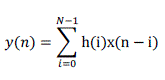 |
||||||||||||||||||||||||
| Where, N represents the filter order. Here BP FIR filter of order 17 is designed using Kaiser window. As we see from the above equation for a filter of order N, the number of adders required is N. The number of multipliers and filter coefficients required will be (N+1). | ||||||||||||||||||||||||
B. DISTRIBUTED ARITHMETIC |
||||||||||||||||||||||||
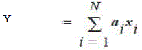
| Distributed arithmetic is an efficient procedure for computing inner products between a fixed and a variable data vector. | ||||||||||||||||||||||||
| Consider the sum-of-products | ||||||||||||||||||||||||
 |
||||||||||||||||||||||||
| where the coefficients, ai, i = 1, 2, ..., N are fixed. | ||||||||||||||||||||||||
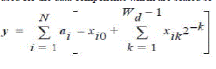
| A 2’s-complement representation is used for the data components which are scaled so that |xi |≤1. | ||||||||||||||||||||||||
 |
||||||||||||||||||||||||
| Where, xik is the kth bit in xi. | ||||||||||||||||||||||||
| Wd is the input bit width. | ||||||||||||||||||||||||
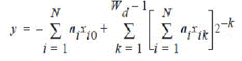
| By interchanging the order of the two summations we get | ||||||||||||||||||||||||
 |
||||||||||||||||||||||||
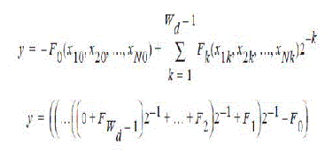
| which can be written as | ||||||||||||||||||||||||
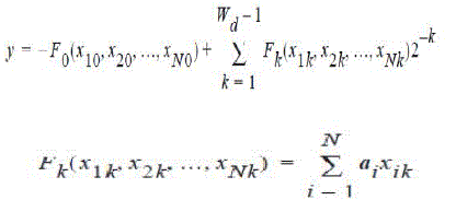 |
||||||||||||||||||||||||
| Where, | ||||||||||||||||||||||||
| F is a function of N binary variables, the ith variable being the kth bit in the data xi. Since Fk can take on only a finite number of values, 2N, it can be computed and stored in a look-up table. This table can be implemented using a ROM (Read-Only Memory). Using Horner’s method for evaluating a polynomial for x = 0.5, we can rewrite | ||||||||||||||||||||||||
 |
||||||||||||||||||||||||
| Inputs, x1, x2,…, xN are shifted bit-serially out from the shift registers with the least-significant bit first. Bits xik are used as an address to the ROM storing the look-up table. | ||||||||||||||||||||||||
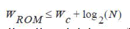
| The computational time is Wd clock cycles. The word length in the ROM, WROM, depends on the Fk with the largest magnitude and the coefficient word length, Wc, and | ||||||||||||||||||||||||
 |
||||||||||||||||||||||||
| The shift-accumulator must be able to add correctly the largest possible value obtained in the accumulator register and in the ROM. The largest value in the accumulator register is obtained when the largest (magnitude) value stored in the ROM is repeatedly accumulated. | ||||||||||||||||||||||||
 |
||||||||||||||||||||||||
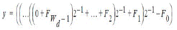
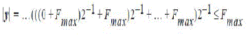
| Thus, at the last clock cycle, corresponding to the sign bit, the value in register y is | ||||||||||||||||||||||||
 |
||||||||||||||||||||||||
| Hence, the shift-accumulator must be able to add two numbers of magnitude ≤Fmax. The necessary number range is ± 1. The word length in the shift-accumulator must be extended with guard bits for overflow detection. Hence, DA is bit serial in nature. It performs bit level rearrangement of MAC operation. It hides explicit multiplication by LUTs. Distributed Arithmetic unit essentially consists of adders augmented by a ROM. | ||||||||||||||||||||||||
| For a filter of order 17 by applying LUT partitioning method number of memory locations required is reduced from 218 to (3*26). | ||||||||||||||||||||||||
IMPLEMENTATION DETAILS |
||||||||||||||||||||||||
| FIR filter implementation involves the following 5 steps: | ||||||||||||||||||||||||
| 1. Filter specification. | ||||||||||||||||||||||||
| 2. Coefficient calculation. | ||||||||||||||||||||||||
| 3. Synthesis and Simulation. | ||||||||||||||||||||||||
| 4. Implementation. | ||||||||||||||||||||||||
| 5. Verification. | ||||||||||||||||||||||||
| A reference model is generated using MATLAB simulink library for the desired filter specifications. The model is verified by giving a sine wave input. The design is synthesized using Xilinx ISE 14.2. The design is simulated using MODELSIM and ISim simulators. Implemented on Virtex-5 FPGA and verified using Chipscope pro. | ||||||||||||||||||||||||
A. DESIGN INDEX OF BANDPASS FILTER |
||||||||||||||||||||||||
| Order: 17 | ||||||||||||||||||||||||
| Sampling frequency: 8MHz | ||||||||||||||||||||||||
| Lower cutoff frequency: 2MHz | ||||||||||||||||||||||||
| β: 0.5 | ||||||||||||||||||||||||
| Pass band gain: 12dB | ||||||||||||||||||||||||
| Stop band attenuation: 6dB | ||||||||||||||||||||||||
| Input data bit width: 16 bits | ||||||||||||||||||||||||
| Output data bit width: 33 bits | ||||||||||||||||||||||||
| Here the sampling frequency is selected according to Nyquist criteria. Hence sampling frequency must be greater than 2 times the cutoff frequency. It will pass only those frequencies in the range 2 to 3.5MHz. | ||||||||||||||||||||||||
| Here Kaiser window is being used for coefficient calculation. As it exhibits less attenuation in stop band region. Stop band attenuation can be controlled by varying β. | ||||||||||||||||||||||||
B. FILTER COEFFICIENTS |
||||||||||||||||||||||||
| Coefficients for BPF of order 17 are designed for Kaiser window using FDA tool for the required specifications. | ||||||||||||||||||||||||
| h(0)= ef84, h(1)= 12f2, h(2)= fe5f, h(3)= fda1, h(4)= ee99, h(5)= 0cc9, h(6)= 2c5c, h(7)= a59c, h(8)= 3051, h(9)= 3051, h(10)= a59c, h(11)= 2c5c, h(12)= 0cc9 , h(13)= ee99 , h(14)= fda1, h(15)= fe5f, h(16)= 12f2, h(17)= ef84. | ||||||||||||||||||||||||
| From the above coefficient values we see that the designed filter is a type1 FIR filter. Hence the filter is of even symmetry with even length. | ||||||||||||||||||||||||
C. TOP MODULE AND MODULE PARTITIONING OF FIR FILTER |
||||||||||||||||||||||||
| The above figure represents the top module of the designed FIR filter. Input,’ filter_in’ is of 16-bit wide. ‘clk’ represent the clock input whose frequency is same as sampling frequency. ‘reset’ should be initially high so that the accumulator content will be initially reset, later it can accumulate the result corresponding to present filter input. ‘clk_enable’ must be high so that ‘clk’ input is enabled. ‘filter_out’ is a 33-bit output, it contain the result of MAC operation. Filter coefficients are 16-bit wide and will be stored in ROM LUTs. | ||||||||||||||||||||||||
| Different blocks in the FIR filter module are, | ||||||||||||||||||||||||
| Delay line: The parallel input data is serialized using pipelined registers contained in the delay line. The input is 16 bit wide and the filter order is 17. Hence the total number of pipelined registers is 16*17=272. | ||||||||||||||||||||||||
| Pre-adder: If the filter is symmetric, the pre-adder is implemented, that reduces by two the number of processed data after delay line. | ||||||||||||||||||||||||
| Transposition module: Performs rearrangement of data. The rearranged data contains bits that have similar weights, but coming from different samples. | ||||||||||||||||||||||||
| ROM LUTs: Contains the pre-computed inner product terms. The transposition module output points to one of the memory locations in the ROM LUTs. | ||||||||||||||||||||||||
| Shift accumulator: Calculates the sum of products obtained from different LUTs. | ||||||||||||||||||||||||
RESULTS |
||||||||||||||||||||||||
A. IMPULSE RESPONSE |
||||||||||||||||||||||||
| It contains 18 samples which represents filter coefficients. | ||||||||||||||||||||||||
B. SIMULINK RESULT |
||||||||||||||||||||||||
| The reference module generated using simulink library is verified by giving a sine wave input of amplitude 5 and frequency 3MHz. Sampled at the rate of 11 samples per μs. | ||||||||||||||||||||||||
C. SIMULATION AND VERIFICATION RESULTS |
||||||||||||||||||||||||
| The final result will be obtained after 272 clock pulses in case of DA based filter. In case of fully parallel architecture output will be obtained after 17 clock pulses. | ||||||||||||||||||||||||
D. IMPLEMENTATION AND VERIFICATION |
||||||||||||||||||||||||
| The synthesized result is implemented on Virtex-5 FPGA. Then it is verified using the insystem debugging tool called chipscope pro. | ||||||||||||||||||||||||
| FPGA Editor is used to perform placement and routing manually. When the design is changed manually, the new location constraints for the swapped components must be added to the User Constraints File (UCF). This ensures that changes are retained when the design is re-implemented. | ||||||||||||||||||||||||
| The ChipScope™ Pro tool assists in working at the Printed Circuit Board (PCB) level. This software embeds logic analyzer core(ILA) and logic controller(ICON) into the design, which allows to view the internal signals and nodes in an FPGA. The ChipScope Pro tool supports user-selectable data channels from 1 to 256. FPGA Editor is used to add or remove nets from these cores. | ||||||||||||||||||||||||
| The Integrated Controller (ICON) core provides the communication between the embedded ILA and the computer running the ChipScope Pro Analyzer software. | ||||||||||||||||||||||||
| The ILA core is a customizable logic analyzer core that can be used to monitor the internal signals in the design. Because the ILA core is synchronous to the design being monitored, all design clock constraints applied to the design are also applied to the components inside the ILA core. As the FFGA kit contain only 13 input pins. As the input is 16-bit wide a ROM block has to be inserted. The ROM block contain the input which will be retrieved through a counter. The input to the counter is clock. The output from counter points to one of the ROM locations. The data present in this location will be the input to filter block. The filter output is given to ILA. The output is observed in chicpscope pro analyzer window. | ||||||||||||||||||||||||
| Hence we see that ‘1FFFAB51E’ is the output for the input ‘00AF’. | ||||||||||||||||||||||||
E. DESIGN SUMMARY |
||||||||||||||||||||||||
a. Area and resource utilization report: |
||||||||||||||||||||||||
| Total memory usage of the design using DA architecture is 222,384 kilobytes. Total memory usage using fully parallel architecture is 283,120 kilobytes. Hence optimal resource utilization is seen in case of DA. | ||||||||||||||||||||||||
| DA-based filter requires less area when compared to its MAC counterparts because it doesn't require multipliers. In DA architecture the number of fully utilized LUT flip flop pair increases . Hence resource utilization increases . | ||||||||||||||||||||||||
b. Timing report: |
||||||||||||||||||||||||
| 1. Timing report for DA architecture: | ||||||||||||||||||||||||
| Minimum period: 6.699ns (Maximum Frequency: 149.276MHz) | ||||||||||||||||||||||||
| Minimum input arrival time before clock: 3.326ns | ||||||||||||||||||||||||
| Maximum output required time after clock: 3.259ns | ||||||||||||||||||||||||
| Maximum combinational path delay: No path found | ||||||||||||||||||||||||
| Total REAL time to Xst completion: 14.00 secs | ||||||||||||||||||||||||
| Total CPU time to Xst completion: 13.31 secs. | ||||||||||||||||||||||||
| 2. Timing report for fully parallel architecture: | ||||||||||||||||||||||||
| Minimum period: 12.642ns (Maximum Frequency: 79.101MHz) | ||||||||||||||||||||||||
| Minimum input arrival time before clock: 1.548ns | ||||||||||||||||||||||||
| Maximum output required time after clock: 3.259ns | ||||||||||||||||||||||||
| Maximum combinational path delay: No path found | ||||||||||||||||||||||||
| Total REAL time to Xst completion: 21.00 secs | ||||||||||||||||||||||||
| Total CPU time to Xst completion: 20.80 secs. | ||||||||||||||||||||||||
c. Power report: |
||||||||||||||||||||||||
| Total power consumed using DA is 1.045W. Using fully parallel architecture it is 1.046W. Hence a power reduction of 1mW is observed, this is due to the reduction in dynamic power. | ||||||||||||||||||||||||
CONCLUSION |
||||||||||||||||||||||||
| The proposed design uses DA to reduce the number of multipliers required at the expense of additional adders. Exchanging multipliers with adders is advantageous because adders weigh less than multipliers in terms of silicon area. In addition the overhead from the increase in adders in preprocessing and post processing blocks stay fixed, not increasing along with the length of the FIR filter, whereas the number of reduced multipliers increases along with the length of the FIR filter. | ||||||||||||||||||||||||
| An area efficient and hence less power consuming band pass FIR filter can be designed using DA and FPGA. | ||||||||||||||||||||||||
Tables at a glance |
||||||||||||||||||||||||
|
||||||||||||||||||||||||
Figures at a glance |
||||||||||||||||||||||||
|
||||||||||||||||||||||||
References |
||||||||||||||||||||||||
|


