International Journal of Advanced Research in Electrical, Electronics and Instrumentation Engineering
ISSN ONLINE(2278-8875) PRINT (2320-3765)
ISSN ONLINE(2278-8875) PRINT (2320-3765)
| Nimmy Joseph Assistant Professor, Dept. of Electrical and Electronics Engineering, Dayananda Sagar Academy of Technology and Management, Bangalore, India |
| Related article at Pubmed, Scholar Google |
Visit for more related articles at International Journal of Advanced Research in Electrical, Electronics and Instrumentation Engineering
This paper aims to improve the efficiency of a dc-dc buck converter. It enables a synchronous rectifier buck converter to realize zero voltage switching in light load condition. The replacement of output rectifier diode by MOSFET can minimize conduction losses and increase the efficiency of the circuit. The control technique introduced in this paper enables a SR buck converter to carry out ZVS in light load condition to increase efficiency. No extra auxiliary switches or RLC passive components are required. It is of low cost and easy to control
Keywords |
||||||||||||||||||||||||||||||||||||
| Buck converter, synchronous rectifier, ZVS, light load condition. | ||||||||||||||||||||||||||||||||||||
INTRODUCTION |
||||||||||||||||||||||||||||||||||||
| Buck converters have already been applied to portable products which are powered by batteries. The efficiency of a buck converter should be increased to prolong the operation of portable products and minimize battery drain. The efficiency of a buck converter is affected by conduction losses. Switching loss of a buck converter must be decreased in light load condition. In order to reduce the conduction losses and raise the efficiency the SR technique is used. | ||||||||||||||||||||||||||||||||||||
| In fig.1the basic circuit diagram of synchronous rectifier buck converter to have ZVS in light load condition is shown. A new control technique is proposed in this paper. It enables a SR buck converter to have ZVS function and increase efficiency in light load condition without the need for extra auxiliary switches or RLC passive components. This new control technique is low cost and easy to control. Because the output rectifier diodes are replaced by MOSFET, conduction loss will be lower and the efficiency of the whole circuit will be higher. Fig. 1 shows the circuit topology of a SR buck converter [1]-[4]. | ||||||||||||||||||||||||||||||||||||
OPERATING PRINCIPLES |
||||||||||||||||||||||||||||||||||||
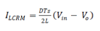
| The oscillogram of the inductor current and switches when the SR buck converter is operated in critical-conduction mode (CRM) is shown in Fig. 2. In CRM, the average inductive current IL of a SR buck converter can be represented by Equation (1), where TS stands for switching frequency and D For duty cycle. | ||||||||||||||||||||||||||||||||||||
 |
||||||||||||||||||||||||||||||||||||
| In the equation, the SR buck converter is operated in discontinuous conduction mode (DCM) if the mean value of the output current IO is lower than ILCRM. However, TS, Vin, VO, L, and D remain unchanged. It is operated in a continuous conduction mode (CCM) if the mean value of the output current IO is higher than ILCRM. Based on the descriptions above analysis, Equation (1) determines which mode the converter will be operated in, whether DCM or CCM. | ||||||||||||||||||||||||||||||||||||
| In fig.2. the oscillogram of the inductor current and voltage across the switches are shown. | ||||||||||||||||||||||||||||||||||||
| Two assumptions are made as follows to simplify the analysis: | ||||||||||||||||||||||||||||||||||||
| 1. The output voltage is assumed as a constant-voltage source because the output capacitance is large enough | ||||||||||||||||||||||||||||||||||||
| 2. That no losses arise from any parts in the circuit is assumed. All the components are assumed to be ideal. | ||||||||||||||||||||||||||||||||||||
A .Modes of operations in light load |
||||||||||||||||||||||||||||||||||||
| State 1(t0~t1): | ||||||||||||||||||||||||||||||||||||
| In this state, the main switch Q1 is conducted, whereas the SR switch Q2 is off. The input current iin flows through the inductor to the load. The conduction path is shown in Fig. 3(a). The inductor L is charged by Vin -VO at this time, whereas the inductor current iL(t) begins to increase linearly. The inductor current equation is | ||||||||||||||||||||||||||||||||||||
| State 2 (t1~t2) | ||||||||||||||||||||||||||||||||||||
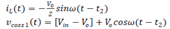
| In State 2, the main switch Q1 is turned off, whereas the Q2 is conducted. The conduction path is shown in Fig. 3(b). As the inductor current is continuous, it flows through Q2 to avoid the breakage of inductor current. The inductor L is discharged by -VO at this time, and the inductor current iL begins to decrease linearly. The inductor current equation in this state is | ||||||||||||||||||||||||||||||||||||
| and the parasitic capacitor voltage equation is | ||||||||||||||||||||||||||||||||||||
| State 3 (t2~t3): | ||||||||||||||||||||||||||||||||||||
| The inductor current has already dropped to 0 at t2. The SR switch Q2 is turned off to avoid energy losses of the buck converter. The conduction path is shown in Fig. 3(c). In this state, the inductor L start to resonant with the parasitic capacitor Coss of switch Q1 and Q2, this enables Coss1 to be discharged and Coss2 to be charged. The iL(t) and vCoss1 can be calculated as follows: | ||||||||||||||||||||||||||||||||||||
 |
||||||||||||||||||||||||||||||||||||
| Where | ||||||||||||||||||||||||||||||||||||
| State 4 (t3~t4) | ||||||||||||||||||||||||||||||||||||
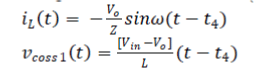
| In State 4, the switch Q1 keeps turning off, whereas the SR switch Q2 is conducted. The conduction path is shown in Fig. 3(d). As a result, the inductor voltage is vL=-VO, this enables the inductor L to be charged and the inductor current to increase linearly in the opposite direction. The current iL(t) at this time is | ||||||||||||||||||||||||||||||||||||
| The parasitic capacitor voltage vCoss1(t) of switch Q1 is | ||||||||||||||||||||||||||||||||||||
| State 5 (t4~t5) | ||||||||||||||||||||||||||||||||||||
| State 5 is the duration for resonance. The switch Q1 and the SR switch Q2 are both turned off. The conduction path is shown in Fig. 3(e). The SR rectifying switch is turned off, whereas the inductor current must be continuous. This current will discharge to Coss1 and charges to Coss2 until the voltage of Coss1 is discharged to 0, and the voltage of Coss2 is charged from 0 to Vin. The iL(t) and vCoss1(t) of switch Q1 are calculated as follows: | ||||||||||||||||||||||||||||||||||||
 |
||||||||||||||||||||||||||||||||||||
| State 6 (t5~t6) | ||||||||||||||||||||||||||||||||||||
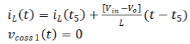
| In State 6, the main switch Q1 and the SR switch Q2 are continuously turned off. However, Coss1 has been discharged, and Coss2 has been discharged by inductor current. The body diode D1 is then conducted. The conduction path is shown in Fig. 3(f). In this state, the zero voltage condition of Q1 has been completed. The iL(t) and vCoss1(t) of switch Q1 are calculated as follows: | ||||||||||||||||||||||||||||||||||||
 |
||||||||||||||||||||||||||||||||||||
| In fig,3(a)-(f) the six operation states of the control technique for the synchronous rectifier buck converter proposed in this paper is shown. According to the previous description, the SR buck converter is operated in DCM in light load condition. When the inductor current is lower than 0, the SR switch Q2 remains to be turned on. That will result in the decrement in conversion efficiency of the SR buck converter. The second conduction of SR switch Q2 in one switching cycle enables the main switch Q1 to be turned on with ZVS and increase the efficiency in light load condition. In conclusion, the control technique proposed in this paper has the following advantages. When the SR buck converter is operated in heavy load condition, the SR technique can be used to reduce conduction losses. In contrast, the ZVS technique can be adopted in light load condition to reduce switching losses. | ||||||||||||||||||||||||||||||||||||
B. Conditions for ZVS in light load condition |
||||||||||||||||||||||||||||||||||||
| To attain the ZVS of main switch Q1 in light load condition, the inductor L must store enough energy to let the parasitic capacitor of switch Q1 be discharged completely in State 4. Therefore, the energy EL stored by inductor has to be higher than ECoss1 stored by capacitor. This can be represented by the following equation (iLp) is the peak value of inductor current): | ||||||||||||||||||||||||||||||||||||
| The pulse duration for State 4 can be calculated using Equation | ||||||||||||||||||||||||||||||||||||
| In order to attain the ZVS of switch main Q1, the switch Q1 in State 6 must be conducted. If the Q1 is not conducted, the inductor current will charge to Coss1 again in the positive direction, thus the ZVS of main switch Q1 may fail. The delay time from State 5 to State 6 is critical to the ZVS function of main switch Q1. The optimal delay time is 1/4 of the resonance cycle. It is represented by the following equation: | ||||||||||||||||||||||||||||||||||||
SIMULATION MODEL AND RESULTS |
||||||||||||||||||||||||||||||||||||
| The proposed DC-DC converter is simulated using MATLAB and the results are presented here. | ||||||||||||||||||||||||||||||||||||
| In fig.4. the control circuit structural diagram of a synchronous rectifier buck converter is shown. The circuit simulated in MATLAB is given. | ||||||||||||||||||||||||||||||||||||
| In fig. 5. and fig. 6. the open loop and closed loop control of synchronous rectifier buck converter is shown. The circuit is simulated in MATLAB. | ||||||||||||||||||||||||||||||||||||
| In fig.7 and fig. 8 the input voltage of 12 V and output voltage for open loop control is shown. The output is shown in MATLAB SIMULINK. | ||||||||||||||||||||||||||||||||||||
| In fig.9 pulses which are given for main switch and in fig.10 pulses which are given for SR switch is shown. | ||||||||||||||||||||||||||||||||||||
| In fig.11 the input current of closed loop control and in fig.12 output current of closed loop control circuit is shown. | ||||||||||||||||||||||||||||||||||||
| In fig.13 output voltage of closed loop control i.e 5V is shown. The output is shown in MATLAB SIMULINK. | ||||||||||||||||||||||||||||||||||||
| In table I the model parameters of all the components are given for both simulation and hardware. The switching frequency is 100kHz. Simulation has done in MATLAB SIMULINK. | ||||||||||||||||||||||||||||||||||||
HARDWARE IMPLEMENTATION |
||||||||||||||||||||||||||||||||||||
| The test setup of the hardware was realized. Individual modules were tested and then integrated. The experimental setup and the various waveforms are as shown below. | ||||||||||||||||||||||||||||||||||||
| In fig.14 The experimental hardware setup for the prototype is shown. One diode is replaced by MOSFET to reduce the conduction losses. | ||||||||||||||||||||||||||||||||||||
A. Hardware Results: |
||||||||||||||||||||||||||||||||||||
| The synchronous rectifier buck converter for ZVS in light load condition has been modeled simulated and a prototype for the same is developed. | ||||||||||||||||||||||||||||||||||||
| In fig.15 the output voltage of 5V for hardware is shown and in fig.16 the pulses for main switch which is given in hardware is shown. | ||||||||||||||||||||||||||||||||||||
| Figure 16 and 17 shows the pulses for main switch and the SR switch. Figure 18 shows the Zero Voltage Switching across auxiliary switch got in hardware. | ||||||||||||||||||||||||||||||||||||
CONCLUSION |
||||||||||||||||||||||||||||||||||||
| In this paper, the control technique applicable to a SR buck converter is proposed, and the analysis of its operating principles is discussed. The control method proposed herein has two advantages. First, due to the SR technique proposed in the paper, the diode of output rectifier can be replaced by a MOSFET. This will help to reduce conduction losses and increase the conversion efficiency of the converter. Second, when the converter is operated in light load condition, ZVS will be achieved successfully without any auxiliary switch or passive component(R, L, C). In other words, there is no need to add extra cost in the converter, and the conversion efficiency of the converter can also be increased in light load condition. | ||||||||||||||||||||||||||||||||||||
ACKNOWLEDGMENT |
||||||||||||||||||||||||||||||||||||
| This work was supported by Kerala Electrical and Allied Engineering Co. Ltd. | ||||||||||||||||||||||||||||||||||||
Tables at a glance |
||||||||||||||||||||||||||||||||||||
|
||||||||||||||||||||||||||||||||||||
Figures at a glance |
||||||||||||||||||||||||||||||||||||
|
||||||||||||||||||||||||||||||||||||
References |
||||||||||||||||||||||||||||||||||||
|


