International Journal of Advanced Research in Electrical, Electronics and Instrumentation Engineering
ISSN ONLINE(2278-8875) PRINT (2320-3765)
ISSN ONLINE(2278-8875) PRINT (2320-3765)
G. Krishna Rao1, Bighneswar Panda2, T.Sridhar3
|
| Related article at Pubmed, Scholar Google |
Visit for more related articles at International Journal of Advanced Research in Electrical, Electronics and Instrumentation Engineering
In this paper, our objective is to detail know-how and techniques that can help the designer of electronic circuits to develop and to optimize their own IP in a reasonable time. For this reason, we propose to optimize existing FFT algorithms for low-cost FPGA implementations. For that, we have used short length structures to obtain higher length transforms. Indeed, we can obtain a VLSI structure by using log4(N) 4-point FFTs to construct N-point FFT rather than (N/8) logs (N) 8-point FFTs. Furthermore, two techniques are used to yield with VLSI architecture. Firstly, the radix-4 FFT is modified to process one sample per clock cycle. Secondly, the memory is shared and divided into 4 parts to reduce the consumed resources and to improve the overall latency
Keywords |
| FPGA, 8-pointFFT,4-pointFFT,spatial distribution, temporal distribution. |
INTRODUCTION |
| The Discrete Fourier Transform (DFT) is one of the most important tools used in Digital Signal Processing applications. It has been widely implemented in digital communication systems such as Radars, Ultra Wide Band (UWB) receivers and many other applications. Computing this operation has a high computational requirement and needs a large number of operations (N2 complex multiplications and N. (N -1) complex additions).This makes computing and implementation very difficult to realize. To reduce the number of operations a fast algorithm has been introduced by Cooley-Tukey [1] and called Fast Fourier Transform (FFT).The latter reduces complexity from O (N2) to O (NlogN). Other researchers, propose numerous techniques such asradix-4 [2], split radix [3] to avoid radix-2structure in order to reduce the complexity of FFT algorithm. These architectures are either based on the Decimation-in Time (DIT) or on the Decimation-in-Frequency (DIP). Several designs based on these architectures were proposed in order to implement these algorithms. On the other hand, there is a growing interest in Field Programmable Gate Arrays (FPGAs) because of their potential to substantially accelerate computational intensive algorithms such as FFTs.Unfortunately, high order FFT are almost implemented into high cost FPGAs. For example, it is not possible to instantiate S12-point FFT with the Xilinx IP core to implement it in Spartan 3family. To meet with this challenge, we present in this paper a VLSI architecture to allow the implementation of high order FFT into low cost FPGAs. The remainder of this paper is organized as follows. In section II, definition and two kinds of distributions (spatial and temporal) are introduced. Section III is devoted to the proposed low area architecture. We detail the principle and the structure of 64-point FFT which may be generalized to higher orders. Then, techniques to save area are illustrated. Section IV presents the experimental results and comparisons with IP core and prior works quoted in the literature. Finally, we summarize and conclude this paper in section V. |
BACK GROUND |
| For a given sequence x of n samples, the DFT frequency components X (k) may be defined as |
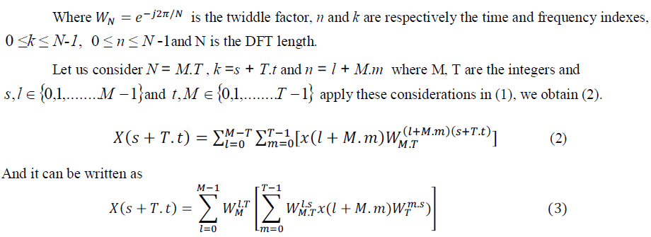 |
| Equation (3) means that it is possible to realize N-point FFT by first decomposing into one M-point and one Tpoint FFT where N = M.T, and then combining them. To illustrate this by example, we take the 64-point as a case study after that we can make generalization to a higher order. To perform 64-point FFT we may choose M = T = 8. Then equation (3) is |
| Equation (4) means that is possible to express the 64- point FFT by two-dimensional structure of 8-point FFT. The processing element of higher order FFT according to equation (3) is the 8-point. Hence, the performance of high length depends in 8-point performance. The choice of 8-point FFT structure becomes crucial. In this work, the 8-point FFT architecture used is the Split Radix DIT because of its lower number of arithmetic operations. |
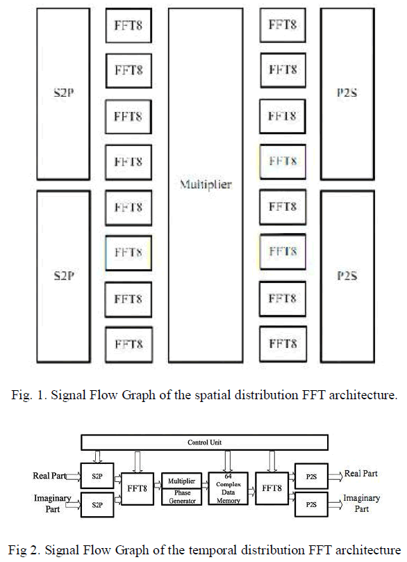
B. Spatial distribution |
| One possible realization of the 64-point FFT is presented in the Signal Flow Graph (SFG) of Fig. 1. It can be observed that computing 64-point FFT is composed on five levels. The first level is composed of two serial to parallel blocks used to store real and imaginary part of data presented in a serial way. The second floor is composed of 8 blocks of 8-point FFT Split Radix DIT. The third block contains 49 complex multipliers used to compute non trivial complex multiplication. The fourth is similar to the second one. The last level is composed of two parallel to serial blocks gives data in a serial way. At the 64th clock cycle all input data are ready to be proceeded. After 5 clock cycles, the 8-point FFT outputs are available and multiplication can be started. Block multiplier needs 2 clock cycles to perform the 49 complex multiplications. |
| The 64-point FFT outputs are available 5 clock cycles after the last stage of 8-point FFT transformation. Hence, the main advantage of this architecture is the high speed and low-latency. However, the implementation of this architecture on FPGA needs high memory, high number of complex multipliers and complex adders. Therefore, this architecture is not suitable for low cost FPGA such as Spartan 3 family. |
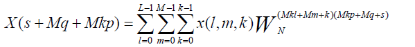
C. Temporal distribution |
| Another possible realization of the 64-point FFT is illustrated in Fig. 2. According to this structure, the first stage is realized by one block of 8-point FFT rather than 8 as in Fig. 1. Similarly, the third stage is performed by only one block of 8-point FFT rather than 8. Consequently, the control unit in Fig. 2 plays an important role to synchronize |
| This architecture performs FFT in a pipeline way. First, input data comes in a serial manner. To perform the computation input data have to be parallelized. This is realized by S2P blocks which are implemented by means of delay registers. On the other side, the control unit manages the input data addresses. The first 8-point input data has the address in the format 8j, j E {O, 1, ... 7}. On the 56th clock cycle these data have been proceeded to the first stage of 8- point FFT. After 5 clock cycles, the 8-point FFT outputs are available and multiplication can be started. Similarly, on the 57th clock cycle, data indexed 8j + 1 will be transformed by the first 8-point FFT and after 7 clock cycles, results data will be available at the multiplier output. And so one until the last result of multiplier output which will be available at the 71st clock cycle. These results are stored on the fly on 64-complex data memory. Likewise, the second 8-point FFT stage will proceed the stored data to compute 64-point FFT. |
 |
D. Compromise analysis |
| Some concluding remarks related to this section have to be drawn. Firstly, decomposing a high length FFT to 8-point FFTs may be done in a spatial or in temporal distribution. In terms of throughput, the two distributions present one complex output per clock cycle since data have to be serialized by P2S component. On the other hand, the latency which represents the elapsed time to get the first result is the same. In fact, for a given N = 8n where n is the number of stages, the latency in both architectures may be expressed as L(N) = N + 7log8(N – 2). The main difference between the two distributions is the consumed area. Obviously, the second architecture consumes averagely 7 times less area than the first one. The number of 8-point FFT blocks pass from 16 to 2 and the number of nontrivial multiplier pass from 49 to 7. Furthermore, the complex data memory used in Fig.2 may be avoided by storing the multiplier Outputs on S2P register. Indeed, since input data at address 8j, 8j+l,.. Are proceeded one can use these addresses to store the multiplier outputs. |
| Definitively, the major drawback of the decomposition of high length FFT on 8-point FFTs is related to the hardware consumed resources of the 8-point FFT. Synthesis results of the split radix DIT description of 8- point FFT show that the percentage of occupied slices in Spartan3E XC3S500 is about 30%. Therefore, to design a higher order FFT, the FPGA resources will be overflowed. Another drawback is about the limitation of the number of input with exclusively 8-point FFT elements since N = 8n. To overcome this problem we replace the 8-point FFT by a 4-point FFT using radix-4 algorithm. This choice is reinforced by the synthesis results of radix 4 in terms of slice occupation which is about 2%. |
LOW AREA ARCHITECURE |
A. Definition |
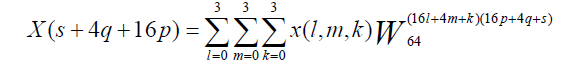
| The N-point FFT equation can be split into three stages according to next equation. |
 |
| For N = 64, one possible solution consists on constructing the 64-point FFT according to the temporal distribution by using 8-point, 4-point FFT and 2-point FFTs. The obtained design is not highly structured and inhomogeneous. The second solution consists in constructing the 64-point FFT by three stages of 4-point FFT. For L = M = K = 4, 64-point FFT equation can be written as |
 |
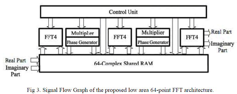
B. Optimizations |
| Using the radix-4 processing element, we can represent the64-point FFT according to SFG in Fig. 3. The 64- point FFT is composed of a control unit, three blocks 4-point FFT units, two blocks multipliers units with two phase generator units and a complex 64-point memory unit. The control unit, indeed of managing the FFf4, multipliers and memorizing unit, it is used also to generate addresses of the inputs and the outputs of each block |
| 1) Radix-4 modification: Outputs of such algorithm are presented in next equations |
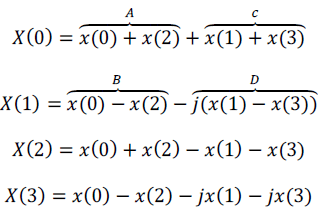 |
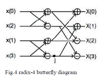
| The SFG of the radix-4 structure is illustrated in Fig. 4. It is shown that radix-4 algorithm is composed of 8 complex additions/subtractions. In order to reduce the number of complex multipliers, after each 4-point FFT and to keep the pipeline way in computation of the design we modify the 4-point FFT architecture. |
 |
| Usually, the radix-4 is computed as multi-inputs multioutputs system. This structure requires 4 multipliers in one clock cycle. It is true that this structure presents a high speed design, but almost a P2S block is used to serialize data. For these reasons, we rectify the architecture in order to have one multiplier per clock cycle. So, the resulting design have one complex input and give one complex output per clock cycle as represented in Fig. 4. Intermediate signals A, B, C and D used in the diagram are indicated to understand the parallel computing. |
| 2) Sharing memory: For each output of the 4-point FFT block the phase generator generates the correspondent twiddle factor and the multiplier unit performs the complex multiplication and stores the result on 64 complex data memory. This last will be reused and shared between all the blocks as it is shown on Fig. 3. |
| Usually, computing 64-point FFT based on 4-point FFT needs 3 complex memories. In our architecture we use only one complex 64-point. Moreover, this memory is divided into four small 16-point complex memories in order to improve the latency. Indeed, the problem behind this consists in using one shared memory with only one writer port. This is impossible since a part of data already saved in the memory are not used. Furthermore, if we use a dual port memory, this will be synthesized as BRAM blocks which are oversize and available in limited number in low cost FPGAs. |
 |
EXPERIMENTAL RESULTS |
A. Synthesis results |
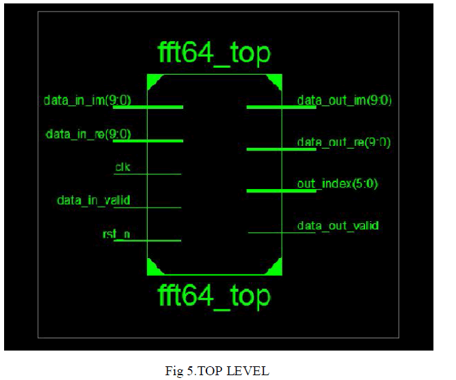 |
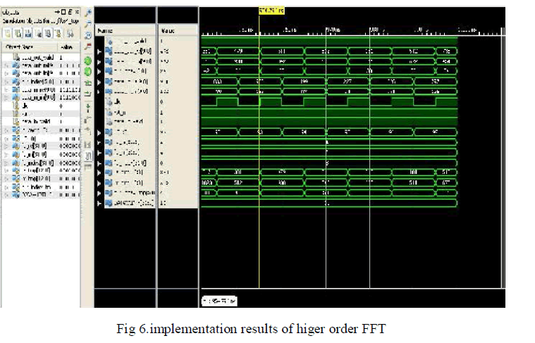
B. Implementation results |
 |
CONCLUSION |
| Techniques to implement high order FFT into low cost FPGAs were presented and validated. After a comprehensive and a comparative study of existing high order FFTs, an optimized architecture of 64-point FFT was proposed. The transition between 64-point and 256-point was exploited. Higher order FFTs could be obtained with the same manner. Our future work for the FPGA implementation will be devoted to the optimization of the block multiplier and the use of the method proposed in [7]to replace embedded multipliers. |
References |
|