International Journal of Advanced Research in Electrical, Electronics and Instrumentation Engineering
ISSN ONLINE(2278-8875) PRINT (2320-3765)
ISSN ONLINE(2278-8875) PRINT (2320-3765)
CH.D.VishnuPriya, C.Srijana Devi
|
| Related article at Pubmed, Scholar Google |
Visit for more related articles at International Journal of Advanced Research in Electrical, Electronics and Instrumentation Engineering
Digital multipliers are among the most critical arithmetic functional units. The overall performance of these systems depends on the throughput of the multiplier. Meanwhile, the negative bias temperature instability effect occurs when a pMOS transistor is under negative bias (Vgs = −Vdd), increasing the threshold voltage of the pMOS transistor, and reducing multiplier speed. A similar phenomenon, positive bias temperature instability, occurs when an nMOS transistor is under positive bias. Both effects degrade transistor speed, and in the long term, the system may fail due to timing violations. Therefore, it is important to design reliable high-performance multipliers. In this paper, we propose an aging-aware multiplier design with a novel adaptive hold logic (AHL) circuit. The multiplier is able to provide higher throughput through the variable latency and can adjust the AHL circuit to mitigate performance degradation that is due to the aging effect. Moreover, the proposed architecture can be applied to a column- or row-bypassing multiplier.
INTRODUCTION |
| Digital multipliers are among the most critical arithmetic functional units in many applications, such as the Fourier transform, discrete cosine transforms, and digital filtering. The through put of these applications depends on multipliers, and if the multipliers are too slow, the performance of entire circuits will be reduced. Furthermore, negative bias temperature instability (NBTI) occurs when a pMOS transistor is under negative bias (Vgs = −Vdd). In this situation, the interaction between inversion layer holes and hydrogen-passivated Si atoms breaks the Si–H bond generated during the oxidation process, generating H or H2 molecules. When these molecules diffuse away, interface traps are left. |
| The accumulated interface traps between silicon and the gate oxide interface result in increased threshold voltage (Vth), reducing the circuit switching speed. When the biased voltage is removed, the reverse reaction occurs, reducing the NBTI effect. However, the reverse reaction does not eliminate all the interface traps generated during the stress phase, and Vth is increased in the long term. Hence, it is important to design a reliable high-performance multiplier. The corresponding effect on an nMOS transistor is positive bias temperature instability (PBTI), which occurs when an nMOS transistor is under positive bias. Compared with the NBTI effect, the PBTI effect is much smaller on oxide/polygate transistors, and therefore is usually ignored. However, for high-k/metal-gate nMOS transistors with significant charge trapping, the PBTI effect can no longer be ignored. In fact, it has been shown that the PBTI effect is more significant than the NBTI effect on 32-nm high-k/metal-gate processes. |
| A traditional method to mitigate the aging effect is overdesign, including such things as guard-banding and gate oversizing; however, this approach can be very pessimistic and area and power inefficient. To avoid this problem, many NBTI-aware methodologies have been proposed. An NBTI-aware technology mapping technique was proposed in to guarantee the performance of the circuit during its lifetime. In an NBTI-aware sleep transistor was designed to reduce the aging effects on pMOS sleep-transistors, and the mlifetime stability of the power-gated circuits under consideration was improved. Wu and Marculescu proposed a point logic restructuring and pin reordering method, which is based on detecting functional symmetries and transistor stacking effects. They also proposed an NBTI optimization method that considered path sensitization. In dynamic voltage scaling and body-basing techniques were proposed to reduce power or extend circuit life. These techniques, however, require circuit modification or do not provide optimization of specific circuits. |
| Traditional circuits use critical path delay as the overall circuit clock cycle in order to perform correctly. However, the probability that the critical paths are activated is low. In most cases, the path delay is shorter than the critical path. For these noncritical paths, using the critical path delay as the overall cycle period will result in significant timing waste. Hence, the variable-latency design was proposed to reduce the timing waste of traditional circuits. The variable-latency design divides the circuit into two parts: 1) shorter paths and 2) longer paths. Shorter paths can execute correctly in one cycle, whereas longer paths need two cycles to execute. When shorter paths are activated frequently, the average latency of variablelatency designs is better than that of traditional designs. For example, several variable-latency adders were proposed using the speculation technique with error detection and recovery. A short path activation function algorithm was proposed in to improve the accuracy of the hold logic and to optimize the performance of the variable-latency circuit. An instruction scheduling algorithm was proposed in to schedule the operations on non uniform latency functional units and improve the performance of Very Long Instruction Word processors. In a variable-latency pipelined multiplier architecture with a Booth algorithm was proposed. In process-variation tolerant architecture for arithmetic units was proposed, where the effect of process-variation is considered to increase the circuit yield. In addition, the critical paths are divided into two shorter paths that could be unequal and the clock cycle is set to the delay of the longer one. These research designs were able to reduce the timing waste of traditional circuits to improve performance, but they did not consider the aging effect and could not adjust themselves during the runtime. A variable-latency adder design that considers the aging effect was proposed. However, no variable-latency multiplier design that considers the aging effect and can adjust dynamically has been done. |
PAPER CONTRIBUTION |
| In this paper, we propose an aging-aware reliable multiplier design with novel adaptive hold logic (AHL) circuit. The multiplier is based on the variable-latency technique and can adjust the AHL circuit to achieve reliable operation under the influence of NBTI and PBTI effects. To be specific, the contributions of this paper are summarized as follows: 1) novel variable-latency multiplier architecture with an AHL circuit. The AHL circuit can decide whether the input patterns require one or two cycles and can adjust the judging criteria to ensure that there is minimum performance degradation after considerable aging occurs; 2) comprehensive analysis and comparison of the multiplier’s performance under different cycle periods to show the effectiveness of our proposed architecture; 3) an aging-aware reliable multiplier design method that is suitable for large multipliers. Although the experiment is performed in 16- and 32-bit multipliers, our proposed architecture can be easily extended to large designs; 4) the experimental results show that our proposed architecture with the 16 × 16 and 32 × 32 column-bypassing multipliers can attain up to 62.88% and 76.28% performance improvement compared with the 16 × 16 and 32 × 32 fixed-latency column-bypassing (FLCB) multipliers. In addition, our proposed architecture with 16 × 16 and 32 × 32 row-bypassing multipliers can achieve up to 80.17% and 69.40% performance improvement as compared with 16× 16 and 32× 32 fixed-latency row-bypassing multipliers. |
PRELIMINARIES |
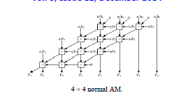
Row-Bypassing Multiplier |
| A low-power row-bypassing multiplier [23] is also proposed to reduce the activity power of the AM. The operation of the low-power row-bypassing multiplier is similar to that of the low-power column-bypassing multiplier, but the selector of the multiplexers and the tristate gates use the multiplicator. |
 |
| Fig. 3 is a 4 ×4 row-bypassing multiplier. Each input is connected to an FA through a tristate gate. When the inputs are 11112 * 10012, the two inputs in the first and second rows are 0 for FAs. Because b1 is 0, the multiplexers in the first row select aib0 as the sum bit and select 0 as the carry bit. The inputs are bypassed to FAs in the second rows, and the tristate gates turn off the input paths to the FAs. |
| Therefore, no switching activities occur in the first-row FAs; in return, power consumption is reduced. Similarly, because b2is 0, no switching activities will occur in the second-row FAs. However, the FAs must be active in the third row because the b3 is not zero. |
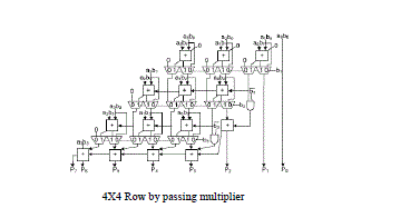 |
| selector of the multiplexer to decide the output of the FA, and ai can also be used as the selector of the tristate gate to turn off the input path of the FA. If ïÿýïÿýïÿýïÿý is 0, the inputs of FA are disabled, and the sum bit of the current FA is equal to the sum bit from its upper FA, thus reducing the power consumption of the multiplier. If ïÿýïÿýïÿýïÿý is 1, the normal sum result is selected. More details for the column-bypassing multiplier can be found. |
VARIABLE-LATENCY DESIGN |
| In ripple carry adders, the carry propagation time is the major speed limiting factor as seen in the previous lesson. |
 |
| Most other arithmetic operations, e.g. multiplication and division are implemented using several add/subtract steps. Thus, improving the speed of addition will improve the speed of all other arithmetic operations. |
| Accordingly, reducing the carry propagation delay of adders is of great importance. Different logic design approaches have been employed to overcome the carry propagation problem. |
| One widely used approach employs the principle of carry look-aheadsolves this problem by calculating the carry signals in advance, based on the input signals. |
| This type of adder circuit is called as carry look-ahead adder (CLA adder).It is based on the fact that a carry signal will be generated in two cases: |
| (1) When both bits A i and B i are 1, or |
| (2) When one of the two bits is 1 and the carry-in (carry of the previous stage) is 1. |
| The Boolean expression of the carry outputs of various stages can be written as follows: |
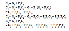 |
| In general, the i th. carry output is expressed in the form |
| In other words, each carry signal is expressed as a direct SOP function of C 0 rather than its preceding carry signal. |
| Since the Boolean expression for each output carry is expressed in SOP form, it can be implemented in two-level circuits. |
| The 2-level implementation of the carry signals has a propagation delay of 2 gates, i.e., 2τ. |
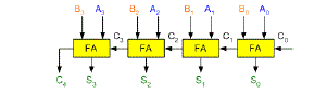
| The 4-bit carry look-ahead (CLA) adder consists of 3 levels of logic: |
| First |
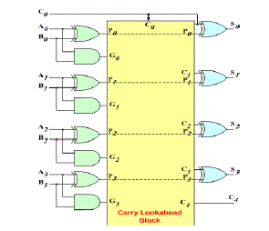 |
| First level: Generates all the P & G signals. Four sets of P & G logic (each consists of an XOR gate and an AND gate). Output signals of this level (P’s & G’s) will be valid after 1τ. |
| Second level: The Carry Look-Ahead (CLA) logic block which consists of four 2-level implementation logic circuits. It generates the carry signals (C 1 , C 2 , C 3 , and C 4 ) as defined by the above expressions. Output signals of this level (C 1 , C 2 , C 3 , and C 4 ) will be valid after 3τ. |
| Third level: Four XOR gates which generate the sum signals (S i ) (S i = P i ⊕ C i ). Output signals of this level (S 0 , S 1 , S 2 , and S 3 ) will be valid after 4τ. |
| Thus, the 4 Sum signals (S 0 , S 1 , S 2 & S 3 ) will all be valid after a total delay of 4τ compared to a delay of (2n+1)ïÃâ¬Ã τ for Ripple Carry adders. |
| For a 4-bit adder (n = 4), the Ripple Carry adder delay is 9τ. |
| The disadvantage of the CLA adders is that the carry expressions (and hence logic) become quite complex for more than 4 bits. |
PROPOSED AGING-AWARE MULTIPLIER |
| The proposed aging-aware reliable multiplier design. It introduces the overall architecture and the functions of each component and also describes how to design AHL that adjusts the circuit when significant aging occurs. |
Proposed Architecture |
| Proposed aging-aware multiplier architecture, which includes two m-bit inputs (m is a positive number), one 2m-bit output, one column- or row-bypassing multiplier, 2m 1-bit Razor flip-flops, and an AHL circuit. |
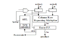 |
| Proposed architecture (md means multiplicand; mr means multiplicator). |
| Hence, the two aging-aware multipliers can be implemented using similar architecture, and the difference between the two bypassing multipliers lies in the input signals of the AHL. According to the bypassing selection in the column or rowbypassing multiplier, the input signal of the AHL in the architecture with the column-bypassing multiplier is the multiplicand, whereas of the row-bypassing multiplier is the multiplicator. |
 |
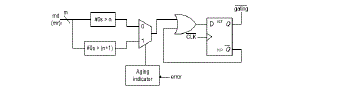 |
| Diagram of AHL (md means multiplicand; mr means multiplicator). |
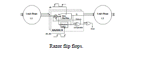
| Razor flip-flops can be used to detect whether timing violations occur before the next input pattern arrives. |
| A 1-bit Razor flip-flop contains a main flip-flop, shadow latch, XOR gate, and mux. The main flip-flop catches the execution result for the combination circuit using a normal clock signal, and the shadow latch catches the execution result using a delayed clock signal, which is slower than the normal clock signal. If the latched bit of the shadow latch is different from that of the main flip-flop, this means the path delay of the current operation exceeds the cycle period, and the main flip-flop catches an incorrect result. If errors occur, the Razor flip-flop will set the error signal to 1 to notify the system to reexecute the operation and notify the AHL circuit that an error has occurred. We use Razor flip-flops to detect whether an operation that is considered to be a one-cycle pattern can really finish in a cycle. If not, the operation is reexecuted with two cycles. Although the reexecution may seem costly, the overall cost is low because the reexecution frequency is low. More details for the Razor flip-flop can be found. The AHL circuit is the key component in the aging-ware variable-latency multiplier. Fig. shows the details of the AHL circuit. The AHL circuit contains an aging indicator, two judging blocks, one mux, and one D flip-flop. The aging indicator indicates whether the circuit has suffered significant performance degradation due to the aging effect. The aging indicator is implemented in a simple counter that counts the number of errors over a certain amount of operations and is reset to zero at the end of those operations. If the cycle period is too short, the column- or row-bypassing multiplier is not able to complete these operations successfully, causing timing violations. These timing violations will be caught by the Razor flip-flops, which generate error signals. If errors happen frequently and exceed a predefined threshold, it means the circuit has suffered significant timing degradation due to the aging effect, and the aging indicator will output signal 1; otherwise, it will output 0 to indicate the aging effect is still not significant, and no actions are needed. The first judging block in the AHL circuit will output 1 if the number of zeros in the multiplicand (multiplicator for the row-bypassing multiplier) is larger than n (n is a positive number, which will be discussed in Section IV), and the second judging block in the AHL circuit will output 1 if the number of zeros in the multiplicand (multiplicator) is larger than n + 1. They are both employed to decide whether an input pattern requires one or two cycles, but only one of them will be chosen at a time. In the beginning, the aging effect is not significant, and the aging indicator produces 0, so the first judging block is used. After a period of time when the aging effect becomes significant, the second judging block is chosen. Compared with the first judging block, the second judging block allows a smaller number of patterns to become one-cycle patterns because it requires more zeros in the multiplicand (multiplicator). The details of the operation of the AHL circuit are as follows: when an input pattern arrives, both judging blocks will decide whether the pattern requires one cycle or two cycles to complete and pass both results to the multiplexer. The multiplexer selects one of either result based on the output of the aging indicator. Then an OR operation is performed between the result of the multiplexer, and the Q¯ signal is used to determine the input of the D flip-flop. When the pattern requires one cycle, the output of the multiplexer is 1. The !(gating) signal will become 1, and the input flip flops will latch new data in the next cycle. On the other hand, when the output of the multiplexer is 0, hich means the input pattern requires two cycles to complete, the OR gate will output 0 to the D flip-flop. Therefore, the (gating) signal will be 0 to disable the clock signal of the input flip-flops in the next cycle. Note that only a cycle of the input flip-flop will be disabled because the D flip-flop will latch 1 in the next cycle. The overall flow of our proposed architecture is as follows: when input patterns arrive, the column- or row-bypassing multiplier, and the AHL circuit execute simultaneously. According to the number of zeros in the multiplicand (multiplicator), the AHL circuit decides if the input patterns require one or two cycles. If the input pattern requires two cycles to complete, the AHL will output 0 to disable the clock signal of the flip-flops. Otherwise, the AHL will output 1 for normal operations. When the column- or row-bypassing multiplier finishes the operation, the result will be passed to the Razor flip-flops. The Razor flipflops check whether there is the path delay timing violation. If timing violations occur, it means the cycle period is not long enough for the current operation to complete and that the execution result of the multiplier is incorrect. Thus, the Razor flip-flops will output an error to inform the system that the current operation needs to be reexecuted using two cycles to ensure the operation is correct. In this situation, the extra reexecution cycles caused by timing violation incurs a penalty to overall average latency. However, our proposed AHL circuit can accurately predict whether the input patterns require one or two cycles in most cases. Only a few input patterns may cause a timing variation when the AHL circuit judges incorrectly. In this case, the extra reexecution cycles did not produce significant timing degradation. In summary, our proposed multiplier design has three key features. First, it is a variable-latency design that minimizes the timing waste of the noncritical paths. Second, it can provide reliable operations even after the aging effect occurs. The Razor flip-flops detect the timing violations and reexecute the operations using two cycles. Finally, our architecture can adjust the percentage of one-cycle patterns to minimize performance degradation due to the aging effect. When the circuit is aged, and many errors occur, the AHL circuit uses the second judging block to decide if an input is one cycle or two cycles. |
SIMULATION RESULTS |
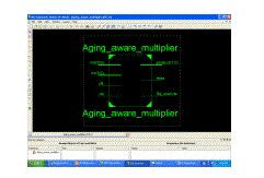
| Block diagram |
 |
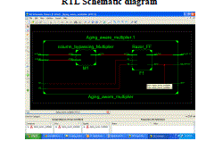
| RTL Schematic diagram |
 |
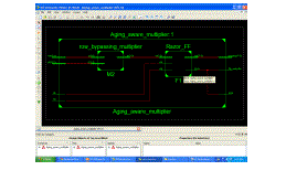
| Technology schematic |
 |
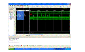
Simulation output waveform |
 |
CONCLUSION |
| This paper proposed an aging-aware variable-latency multiplier design with the AHL. The multiplier is able to adjust the AHL to mitigate performance degradation due to increased delay. The experimental results show that our proposed architecture with 4x4 multiplication with CLA as last stage instead of Normal RCA adder it will decrease the delay and improve the performance compared with previous designs. |
References |
|