International Journal of Advanced Research in Electrical, Electronics and Instrumentation Engineering
ISSN ONLINE(2278-8875) PRINT (2320-3765)
ISSN ONLINE(2278-8875) PRINT (2320-3765)
Anwishta Saha1, Goutam Kumar Panda2 Pradip Kumar Saha3
|
| Related article at Pubmed, Scholar Google |
Visit for more related articles at International Journal of Advanced Research in Electrical, Electronics and Instrumentation Engineering
Generally conventional boost converters have been used to obtain higher output voltage than the input voltage. When these boost converters are operated for high ratios it leads to high voltage and current stress on the switch. Hence an interleaving technique of boost converter has been presented. This method of approach can be used in high power applications to produce high voltage gain when compared to the conventional boost converter. This project report deals with the simulation of Interleaved Boost Converter (ILBC). It is seen that, for higher power applications, more modules can be paralleled to increase the power rating and the dynamic performance. One of the challenges in designing a boost converter for high power application is how to handle the high current at the input side. In this project report an interleaved boost dc-dc converter is proposed for current sharing on high power application. Moreover, this converter also reduces the ripple of voltage. The simulated results are presented with R load.
Keywords |
| Boost converter, Closed loop control, Interleaved, PI controller, Ripple factors. |
I.INTRODUCTION |
| Power converters have required improvement as well as reduction of size and weight especially in mobile information/communication devices, traction converters, power control units for electric/hybrid vehicle, etc. Passive components and cooling devices usually occupy a much larger space than semiconductor devices in power electronics building block. It is well known that when many DGs are connected to utility grids, they can cause problems such as voltage rise and protection problem in the utility grid. To solve these problems, new concepts of electric power systems are proposed [1]. Resonant converters eliminate most of the switching losses encountered in Pulse Width Modulation converters. The active device is switched with either Zero Current Switching or Zero Voltage Switching at its terminals. When current through the switch is made zero, it is turned on /off, it is known as zero current switching and when voltage across the switch is made zero, it is turned on / off, it is known as zero voltage switching [2]. The main objective of this project report is to develop a modular high-efficiency high step-up boost converter with a forward energy-delivering circuit integrated voltage-doubler as an interface for high power applications. In the proposed topology, the inherent energy self-resetting capability of auxiliary transformer can be achieved without any resetting winding. Moreover, advantages of the proposed converter module such as low switcher voltage stress, lower duty ratio, and higher voltage transfer ratio features are obtained [3]. |
| The DC-DC Converter has low switching power losses and high power efficiency. The use of single transformers gives a low-profile design for the step-up DC-DC converter for low-DC renewable energy sources like photovoltaic module and fuel cell [4]. The ILBC converter is gaining its popularity. An Interleaved boost converter usually combines more than two conventional topologies, and the current in the element of the interleaved boost converter is half of the conventional topology in the same power condition. Besides, the input current ripple and output voltage ripple of the interleaved boost converter are lower than those of the conventional topologies. Interleaved boost converters has higher efficiency than the conventional single boost converter [5]. In the interleaved boost converter topology, one important operating parameter is called the duty cycle D. For the boost converter, the ideal duty cycle is the ratio of voltage output and input difference with output voltage [6]. As already well known, the input current and output voltage ripple of interleaved boost dc-dc converter can be minimized by virtue of interleaving operation. Moreover, the converter input current can be shared among the phases, which is desirable for energy dissipation [7]. The features of the interleaved boost dc-dc converter, the principle of operation and the design procedure are discussed in this project report. The simulation and experimental results are presented. |
II.INTERLEAVED BOOST CONVERTER |
| In case of boost converter ripple is present in the input current due to rise and fall of inductor current. This problem can be eliminated by using interleaved boost converter .This technique consists of a phase shifting of the control signals of cells in parallel operating at the same switching frequency. The main advantage are the current distribution .The current in the switches are just a function of the input current .So interleaved boost converters can reduce input current ripple and the switching losses. |
III.ILBC OPERATING PRINCIPLE |
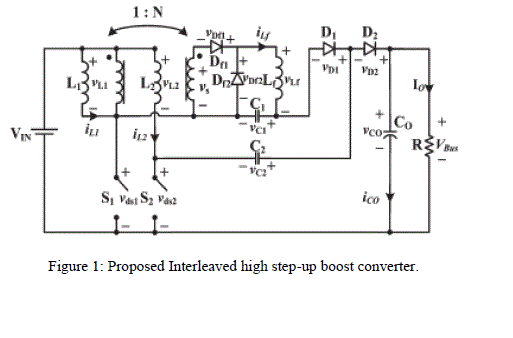
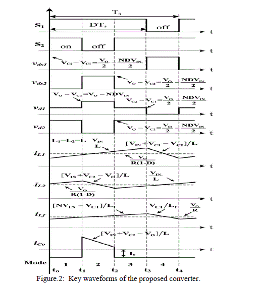
| The proposed interleaved converter topology with high voltage transfer ratio is proposed as shown in Fig.1. The proposed converter consists of two-phase circuits with interleaved operation. The first phase is a boost integrating the forward-type circuit structure, which includes inductor L1 and switch S1 for the boost and an isolated forward energydelivering circuit with turn ratio N. The second phase of the proposed converter is a boost circuit which contains inductor L2, switch S2, blocking capacitor C2, and diode D2 followed by the common output capacitor Co. From Figure.1, one can see that the proposed converter is basically based on the conventional voltage-doubler for the second phase circuit. However, for the first phase, in order to reduce the voltage stress of switch S1 and diode D1, an additional blocking capacitor C1, is added to function as that of C2 for the second phase. The operation principle can be described by considering the key waveforms of the proposed converter as shown in Figure.2. For simplicity, assume that all the components in Figure.1 including the high-frequency transformer of the forward energy delivering circuit are assumed ideal and under steady-state condition. |
 |
 |
IV.MODES OF OPERATION |
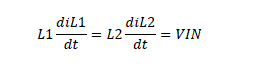
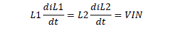
| Mode 1 [t0 < t ≤ t1]: From Fig. 2, one can see that for mode 1, switches S1, S2 are turned on. Diode Df1 is forward biased, while diodes D1,D2,Df2 are reverse biased. During this operation mode, both iL1 and iL2 are increasing to store energy in L1 and L2, respectively. Meanwhile, the input power is delivered to the secondary side through the isolation transformer and inductor Lf to charge capacitor C1. Also, the output power is supplied from capacitor Co. The voltage across inductances L1 and L2 can be represented as follows: |
 |
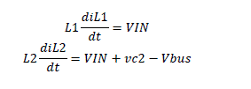
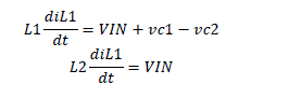
| Mode 2 [t1 < t ≤ t2]: For this operation mode, switch S1 remains conducting, and S2 is turned off. Also, diodes D1 andDf2 remain reverse biased; D2 and Df1 are forward biased. The energy stored in inductor L2 is now released through C2 and D2 to the output. However, the first phase circuit including the forward-type converter remains the same. The voltage across inductances L1 and L2 can be represented as the following: |
 |
| Modes 3 [t2 < t ≤ t3]: For this operation mode, both S1 and S2 are turned on. The corresponding operating principle turns out to be the same as Mode 1. So it can be represented as follows: |
 |
| Mode 4 [t3 < t ≤ t4]: During this operation mode, S1 is turned off, and S2 is turned on. Diode D2 and Df1 are reverse biased, and diode D1 is forward biased. Since diode Df1 is reverse biased, diode Df2 must turn on to conduct the inductor current iLf.. The energy stored in L1 is now released through C1 and D1 to charge capacitor C2 for compensating the lost charges in previous modes. The energy stored in transformer is now treated to perform the selfresetting operation without additional resetting winding. Also, the output power is supplied from capacitor Co. The voltage across inductances L1 and L2 can be represented as follows: |
 |
V.MATLAB SIMULATION |
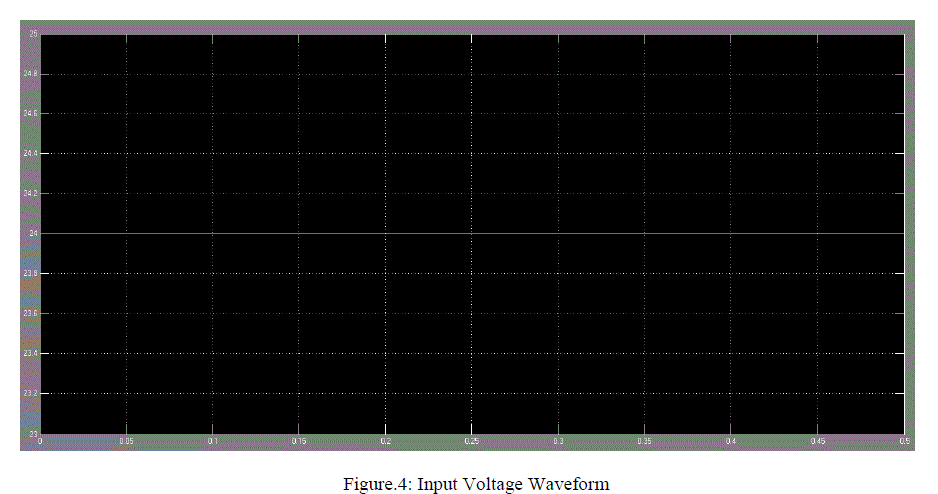
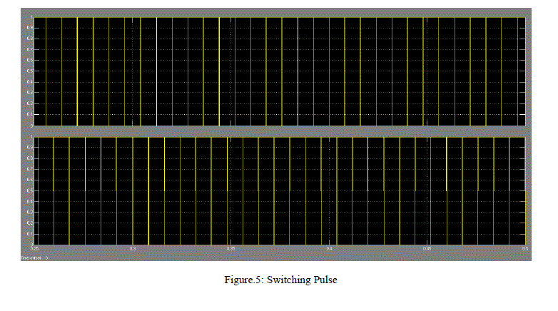
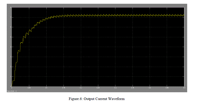
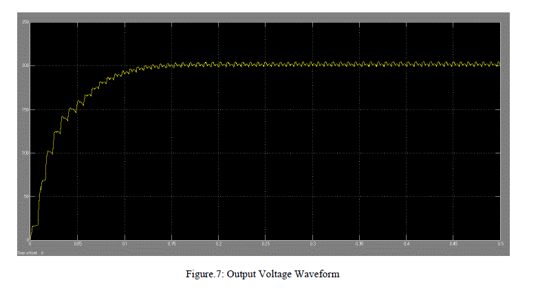
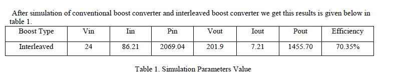
| This is the Simulink diagram of interleaved boost converter with R-Load is shown in Fig.3. The voltage and current measurement blocks are connected to measure the output voltage and output current. The scopes are connected to measure the driving pulse and voltage across the switch. DC input voltage 24v DC is shown in the Figure.4. The gating pulse across the switch is shown in Fig.5. The output current is 7.21Amps and output voltage is 200.9V DC is shown in the Fig.6 and Fig.7. |
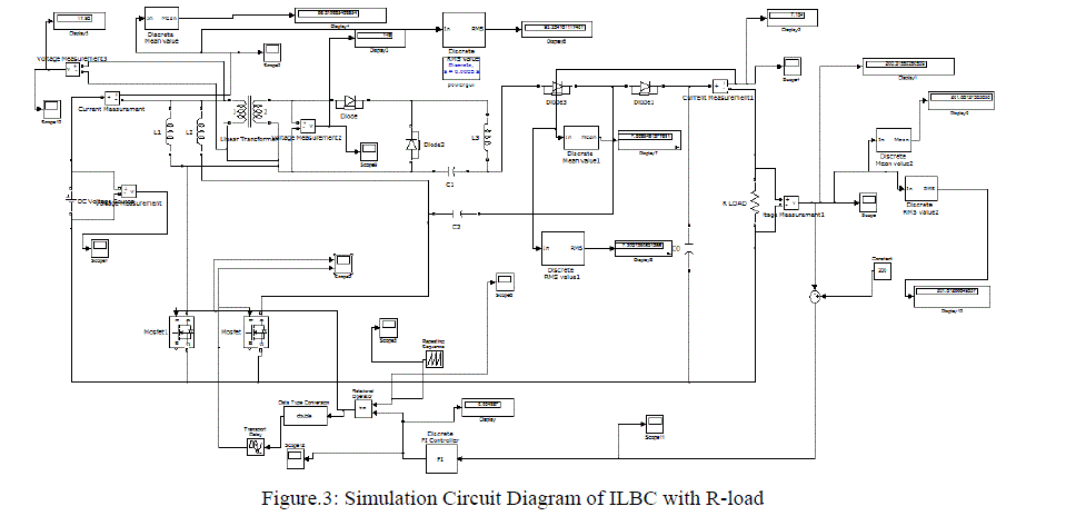 |
| Here the filter capacitor is used to reduce the ripples of the output voltage. The simulation result is given below: |
 |
 |
 |
 |
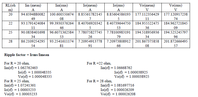
VI.RESULTS |
 |
 |
VII.CONCLUSION |
| High step-up inter leaved boost converter is simulated with R load. The simulation results are in line with predictions. The scope of this work is designing, modeling and simulation of ILBC. The model is developed using the blocks of Simulink. After this we conclude that interleaved boost converter provides high step up voltage 201.9v and high power 1455.70watt. and it is also minimize the ripples of output voltage and current. |
VIII.FUTURE SCOPE |
| A high step-up interleaved boost converter has been simulated in this paper can be simulated with different types of feedback control like fuzzy logic control, genetic algorithm ,artificial neural network and others can be used for power quality improvement or to get high efficiency advanced tuning and to check the constant output voltage with least ripple and to support different appliances with different voltage ratings. |
| Further this simulation model can be hardware implemented for practical output. |
References |
|