International Journal of Advanced Research in Electrical, Electronics and Instrumentation Engineering
ISSN ONLINE(2278-8875) PRINT (2320-3765)
ISSN ONLINE(2278-8875) PRINT (2320-3765)
Musaddeque Anwar Al-Abedin Syed1, Dr. Md. Kamrul Hassan2
|
| Related article at Pubmed, Scholar Google |
Visit for more related articles at International Journal of Advanced Research in Electrical, Electronics and Instrumentation Engineering
There are a number of reasons why light can be used as an efficient carrier of information. As a result, optical communication has gained much importance over the last few decades. The vertical cavity surface emitting laser (VCSEL) is a low cost light source with attractive performance characteristics such as low power consumption, high speed capabilities at low currents, and a circular output beam. These features have madeVCSEL an established component in digital communication networks as the optical source. In this paper, a 1550nm intra-cavity structure Vertical Cavity Surface Emitting Laser (VCSEL) has been designed using quarter nary compound material of AlGaIn Asin both QW and barrier, but with different compositions, and InP as the substrate. Lattice matching has been obtained in the layers from the substrate upto the top contact layer except the quantum well(QW) layers where small amount of compressive strain of 1.6% has been used. AlGaAsSb/AlAsSb has been used as the DBR material for achieving lattice matching with the substrate, and also for achieving higher refractive index contrast. The active material compositions have been chosen to obtain a peak gain at 1550 nm. The out come of this design is a top emitting VCSEL based on In P substrate using a different structure which is capable of producing 1550 nm light output and which can be constructed easily using widely used epitaxial techniques mixed with the MBE using digital alloy technique for the QW layers. The designed VCSEL is successfully simulated as an optical source, with an error free transmission of 70 km through a single mode optical fiber.The finalstructure of the VCSELis alsosuitablefor useinopticalICs.
Keywords |
| Diode Laser, VCSEL, MQW, DBR, 1550nm, AlGaInAs, Optical Source, Optical Fiber Communication |
I.INTRODUCTION |
| Light has numerous characteristics for which it can be used as an efficient carrier of information. First, the high carrier frequency (greater than 100 THz in the so-called communication bands) makes it possible to modulate the signal with enormous amounts of information without significantly affecting the properties of the light. Second, the propagation of the light is highly insensitive to electromagnetic interference, andthird, the short wavelength (∼1 μm) makes it possible to propagate the light in optical fibers. With the development of the semiconductor laser [1], the low loss optical fiber [2, 3], and the fiber amplifier [4], fiber-optics have therefore revolutionized the way people communicate. Long wavelength Vertical Cavity Surface Emitting Lasers (LW-VCSEL)have many advantages such aslow loss in optical fibers, low dispersion for 1.5 μm optical fibers, higher eye safe maximum limit power and lower operation voltages [5].Due to all thesewell-known advantages of VCSELs, current trend has been toreplace the edge emitting lasers by VCSELs [6]. Over the years, the common combination of materials for the quantum well (QW) based semiconductoractive layers have beenGaInAsP/InP, for constructing VCSELs for the 1300nm and 1550nm windows, because of the matchedbandgap of the materials. However, GaInAsP QWs, have lower gain and poor temperature performance than GaAs and InGaAs QWs on GaAs [5]. In case of VCSELs emitting in the 1550nm windows,improvements in various characteristics have been obtained by using AlGaInAs active region, such as a larger conduction band offset than theInGaAsP/InP active region [7], andalsoa better temperature performance than GaInAsP QWs [5].According to Yong et. al. [8],InGaAsN and AlGaInAs have good potential as active layer material systems for low-threshold and high speed modulation bandwidth devices, required for next generation low cost communication links. Thereforein this work, AlGaInAs has been chosen as the active material to get better performance. The design of theVCSEL in this work also utilizes thebenefits of intra cavity structure, which has goodmechanical strength and at the same time is capable ofgood heat dissipation because of heat sinking usingextended metallization [9]. Starting from thesubstrate, bottom DBR mirror |
| system up to the last layer ofthe active region, the VCSEL designed in this work can be grown epitaxially asthe layers are closely lattice matched except theintroduction of small compressive strain in the QWs. The designed VCSEL has shown promising results when simulated as an optical source in an optical fiber communication system employing a single mode optical fiber. |
II. RELATED WORK |
| 1550 nm is a very important wavelength for semiconductor lasers as fiber optic systems have the lowest loss at 1550nm and this wavelength is in the eye safe region for Laser Detection and Ranging (LADAR) applications. Currently, the dominant material system at this wavelength is GaInAsP grown on InP substrates. Although benefiting from twenty years of engineering improvement, the parameters of GaInAsP-based lasers have quite a few limitations when it came to the designing of LW-VCSEL. Therefore, researchers tried to apply the GaAs-based VCSEL structures to long wavelength VCSELs [10–12]. Among the numerous literatures that had been studied, research works carried out by A. Islam et al. [13], Roy et al. [14], Hasan et al. [15] were a few among many that had the similar work, but different results and outcomes to this work. |
III. DESIGN OF THE QUANTUM WELLS |
| The most important aspect of the laser structure design is the active region with strained QWs. When simulating the band structure of strained QWs several factors need to be considered. The transition energy depends on the material composition of the QW, the material composition of the barriers, the width of the quantum well, and the strain of the QW material. |
| AlGaInAsBandgap: The first step in band structure modeling is to get the bandgap of the bulk material. Various interpolation schemes have been proposed to calculate quaternary alloy parameters such as those by Adachi and Vurguftman et al [16, 17]. The simple model was used by Adachi to estimate the optical properties of InPAsSb alloys [16]. In our case, AlGaInAs can be considered as the combination of AlInAs and GaInAs. For the case of latticematched to InP, the ternaries are Ga0.47In0.53Asand Al0.48In0.52As, respectively. The two ternaries (AlInAs andGaInAs) can be derived from the interpolation of three basic binaries (AlAs, GaAs, and InAs). The interpolation formula for ternary is |
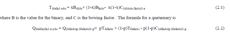 |
| The above interpolation formulas are used to calculate all the parameters of AlGaInAs except the bandgap. This is because, examination of multivariable interpolation formulae shows that all these approaches to III-V quaternary alloy interpolation are arbitrary due to an undetermined multiquadratic term [18].Therefore, a rational approach was developed by Donati to model the compositional dependence of quaternary alloy bandgap using standard multivariable quadratic interpolation [19], in which the biquadratic relationship between quaternary bandgap and binaries can be compacted into a product whose 3x3 matrix includes the alloy parameters. The formula becomes |
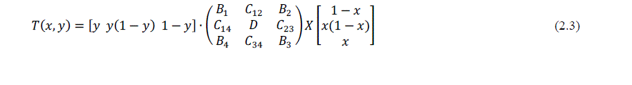 |
| WhereBis are the parameter values of the ith binaries. If Cij and D bowing parameters are zero, Vegard’s law is recovered in its bilinear formulation. One binary can be assigned twice on the same row or column of the alloy matrix with a zero bowing factor (i.e. Alx[GayIn1-y]1-xAs). |
| Band Structure of Strained Layer:The second step in band structure modeling is to include the strain effect.Strain in the semiconductor layer will modify the band structure. In strained devices, a thin layer has different native lattice constant than the surrounding layers. The mismatch of lattice constant will lead to stress and thereby biaxial in-plane strain for this layer. The in-plane strain ε is given by |
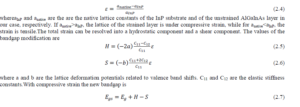 |
IV.DESIGN OF THE DEVICE STRUCTURE |
| Considering all the calculations discussed in the earlier article, a few MATLAB scripts were developed to calculate the required parameters and also to simulate the band structure of strained AlGaInAs QWs on InP substrate. |
| Designing the Active Region and the Cavity: For a laser with an operating wavelength of 1550 nm, the transition energy is |
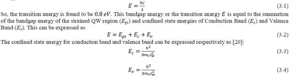 |
| Where, lwis the thickness of the Quantum Well, ���� and ���� are the effective masses of electron in the conduction band and valence band respectively. |
| Adjusting the thickness of the strained QW and it’s alloy composition to target a C-HH transition appropriate to the desired 1550 nm wavelength, i.e. 0.8eV, the thickness of each QW is found to be 8nm and the composition is finalized to be Al0.12Ga0.12In0.76As, having a refractive index of 3.44. |
| Using the knowledge of the basic structure of a top emission VCSEL, the device has been finalized to have a three quantum well structure. To achieve an acceptable band offset, quaternary compound AlxGayIn1-x-yAs lattice matched to InP has been chosen the as the barrier material, with the composition as Al0.3Ga0.17In0.53As. This barrier material produces an energy band gap of 1.21 eV, and has a refractive index of 3.32. The active region has been sandwiched by a layer of Separate Confinement Heterostructure Layer (SCH), that of the same material and composition as the barrier layer. The p-cladding layer on top of the SCH is chosen as Al0.48In0.52As (Si doped), and the n-cladding layer at the bottom of the |
| SCH is chosen as Al0.48In0.52As (C doped), both of which are lattice matched to the substrate, has an energy bandgap of 1.45 eV, and a refractive index of 3.23. The energy gap for this composition of the materials has been computed using the equation [21] |
 |
| InP has been used as the substrate material, whose lattice constant is 5.869 and the refractive index value is 3.18. The barrier, the SCH and the cladding layer, all are fully lattice matched with the substrate. |
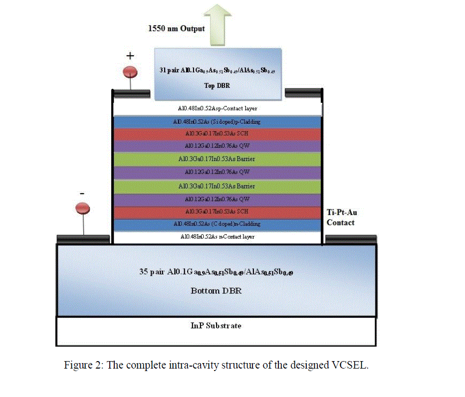
| Designing the DFB Mirrors: For designing the top and bottom DBR mirror system, previous works have been studied and the compound semiconductor combination AlGaAsSb/AlAsSb has been used as the DBR material for achieving lattice matching and also for achieving higher refractive index contrast [13, 22]. But the thermal conductivity of AlGaAsSb/AlAsSb is 3.62 W/m/K [23], which is rather low. |
| For this reason, in this design of 1,550 nm VCSEL, the flow injection current through the DBR layers have been bypassed by using intracavity structure to eliminate heat dissipation in the DBR layers. The DBR mirror system is designed to be made up of numerous pairs of lattice matchedAl0.1Ga0.9As0.51Sb0.49/AlAs0.51Sb0.49. The refractive index of Al0.1Ga0.9As0.51Sb0.49 is 3.51, and that of AlAs0.51Sb0.49 is 3.1 [21]. The thickness of each layer of Al0.1Ga0.9As0.51Sb0.49bragg reflector material has been designed as |
 |
| From a previous work [13], it is seen that the bottom DBR mirror system, designed with 35 pairs of Al0.1Ga0.9As0.51Sb0.49/AlAs0.51Sb0.49 yields a reflectivity of 99.9% and the top DBR mirror system, designed with 31 pairs of Al0.1Ga0.9As0.51Sb0.49/AlAs0.51Sb0.49 yields a reflectivity of 99.4%, enabling the designed VCSEL for top emission. |
| Fixing Cavity Length, Cavity Radius and Cavity Volume and Calculation of Confinement Factor: For this VCSEL, the designed cavity length is taken as 1.5λ i.e., 2,325 nm. Considering the design, the physical thickness of each of the three identical quantum wells has been chosen as 8 nm which corresponds to an electronic thickness of 27.52 nm. The thickness of each of the two identical barrier regions has been chosen as 9 nm and the thickness of each of the two SCH regions as 120 nm, which corresponds to an electronic thickness of29.88 nm and 398.4 nm respectively. The thickness of each of the two identical cladding regions has been chosen as 215 nm which corresponds to an electronic thickness of 694.45 nm. |
| The structure is fully symmetric as a result the QWs are positioned at the antinode of the electric field standing wave pattern. The cavity length, Lcavity is then obtained by adding the thicknesses of all the layers and is found out to be 2328.02 nm, which is very close to 1.5 times of the operating wavelength. The substrate thickness is chosen as 350 μm. |
| After all the simulations and calculations, the structure of the VCSEL is finalized.The energy band and the refractive index values of the finalized structure are shown in Figure 1 and the overall layer by layer structure of the designed VCSEL is presented in Figure 2. |
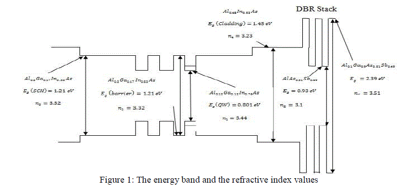 |
| Figure 1 show the energy band and the refractive indices of all the layers used to design the structure of the VCSEL. |
 |
| V. PERFORMANCE CHARACTERISTICS OF THE MODELED VCSEL |
| With the all other threshold parameters found out, the threshold current (Ith) is calculated from [24] |
 |
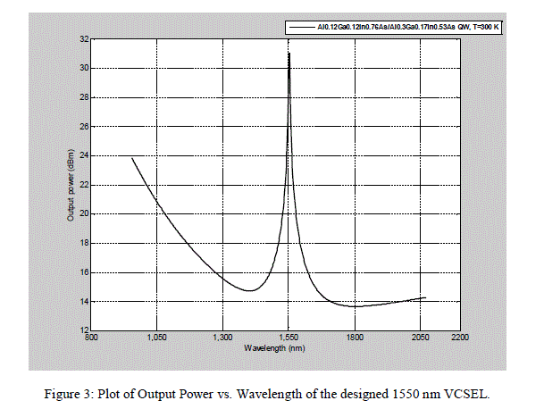
| A MATLAB script is written to simulate the output characteristics of the designed VCSEL, which generates Fig. 3, presenting the performance of the VCSEL in term of its output power. |
 |
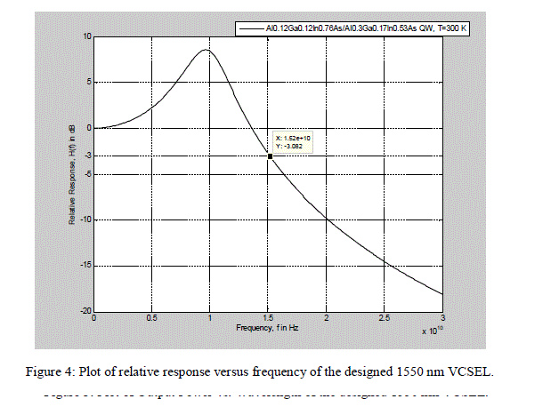
| Using a frequency varying environment of 0 to 26 GHz, the modulation response of the designed lasers has been found out and presented in Figure 4.The small signal analysis gives approximate information about the laser behavior during large signal modulation and as a rule of thumb, the maximum large signal bit-rate is approximately 1.3 times the f3dB when a non-return-to-zero (NRZ) binary modulation format is used [25], i.e. in this case, when the 3dB bandwidth is 15.2 GHz, error free transmission at 19.76Gbit/s, or ~ 20 Gbit/s is possible. |
 |
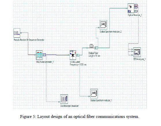
| The simulation tool OptiSystem developed by Optiwave was also used in this work, to design and simulate a real life scenario where the designed VCSEL is used as an optical source in a digital communication network with fiber optics backbone. Figure 5 shows the design of the communication network that has employed the designed 1550 nm VCSEL as an optical source. |
 |
| From Figure 6 and 7, it can be seen that the value of BER<10-12 and the value of Q factor > 7, after the signal is transmitted through 70 km of single mode optical fiber. |
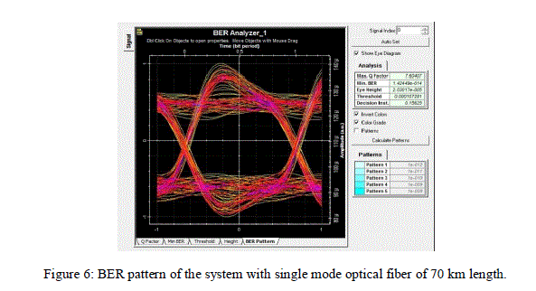 |
| The eye diagram in Figure 6 and Figure 7 is open wide enough to indicate an error free transmission. |
 |
| Some signal degradation occurs due to the attenuation properties of the fiber itself. These values endorse our designed 1550 nm VCSEL as an optical source for an error free transmission at 20 Gbits/s for a maximum of 70 km through a single mode optical fiber without any amplification. |
V. CONCLUSION |
| This work proposes the design with necessary simulations, of a compressively strained MQW Al0.12Ga0.12In0.76As/Al0.3Ga0.17In0.53As on InP substrate for operating as an optical source for optical fiber communication system.The combination of the chosen QW/barrier material has produced satisfactory band offset to provide adequate confinement. Acceptable good contrast in refractive indices of the DBR material could be obtained using quaternary/ternary compound semiconductor pairs in the DBR mirror system.The threshold current for the designed VCSEL, which is desired to be as low as possible, is found to be 0.7 mA, which is very promising. A maximum resonance frequency of 9.6 GHz, is obtained for the designed VCSEL, and the modulation bandwidth is found to be 15.2 GHz. An error free transmission length of 70 km over a single mode fiber, with no amplification, has been obtained when the designed VCSEL was used as an optical source. Analyzing the promising results of different simulations, the VCSEL is expected to perform well if fabricated. |
References |
|