All submissions of the EM system will be redirected to Online Manuscript Submission System. Authors are requested to submit articles directly to Online Manuscript Submission System of respective journal.
A Digital Transponder collects signals in the range of uplink frequencies and transmits them on a different set of downlink frequencies to receivers on Earth. The Transponder consists of RF Receiver; RF Transmitter & digital Baseband Subsystem. In the Digital Baseband Subsystem, the Receiver performs the demodulation of the uplinked command signal down to the data level. The Transmitter linearly phase modulates the Telemetry video signal on a Baseband Transmitter and generates the required RF power before transmission. In this paper, BPSK modulator and demodulator are designed by using VHSIC Hardware Description Language (VHDL) and implemented in Spartan 3E FPGA kit. The Digital Baseband subsystem is used in Spacecraft applications.
Keywords
BPSK, FPGA, Xilinx, Baseband, Transponder, VHDL
I.INTRODUCTION
A digital modulation system is more reliable than analog modulation. The main aim of the paper is to create a BPSK (Binary Phase Shift Keying) modulation and demodulation using Xilinx ISE software in digital baseband subsystem. Binary Phase Shift Keying (BPSK) modulation is widely used modulation scheme in telemetry chain of satellites due to its power efficiency. The modulation scheme employed for telemetry transmission is PCM/BPSK/PM [1]. The BPSK is done at S-band frequencies (2-4) GHz, the BPSK subcarriers are basically at 32 KHz and 128 KHz. The digital modulation technique can be said to be the unpretentious form of phase modulation and is identified as binary because the carrier phase epitomizes only two phase 0âÃÂðand 180°. It is habitually used for high speed data transfer application, and is forceful and simple in the implementation [2].
Digital modulator is the method by which digital symbols are transmitted into waveforms that are suited with the appearances of the channel. The BPSK modulation technique is humblest and most vigorous of all PSK modulation techniques since it takes the highest level of noise or distortion to make the demodulator reach an incorrect decision. It is, however, only able to modulate at 1 bit/symbol and so is unsuitable for high data-rate applications [2], [3], [4], [7].In BPSK modulation the phase of the carrier signal is varied according to the modulating signal. In BPSK modulation the output of logic 0 is phase shifted at lower level and logic 1 is phase shifted at upper level [3]. Depending on the logical condition of the digital input, the carrier is transferred to the output, either in phase or at 180° out of phase, with the reference carrier oscillator. The input signal to the multiplexer can be +cos (ωt) or –cos (ωt).The major advantages of using digital modulation technique are that the use of digital signals diminishes hardware, noise and interference hitches as compared to the analog signal. In Baseband Subsystem BPSK modulation and demodulationused for transmitting and Receiving the signal.
II.RELATED WORK
Anshuman Sharma et al.deliberates that the BPSK demodulator were executed on ALTERA platform. The BPSK demodulator in this work is programmability but the higher clock requirement of 32.256 MHz can still be further enhanced to a lower clock if the FIR filter i.e. Kaiser filter in the demodulator front end is implemented with further parallelism and also the bit synchronizer is prepared to work with precisely two samples per bit [1].
Shruti Helonde et al. had implemented the BPSK modulator in Simulink it has two sine wave generator, a binary data source and a switch. According to the second input, first and third input is controlled. If the second input is logic 0 then sine wave is the output of the switch and if the input is logic1 then output is 180 degrees phase shifted sine wave. The modulated signal added with noise arrives at the input to the BPSK Demodulator [2].
Pratik. A et al. confers the BPSK System implemented on the Spartan 3E Starter Kit board has the same principle as the implementation in System Generator. Although System Generator has an option to generate the VHDL code, for this design the code was made from the beginning because the generated code was hard to read. The only difference was that of the carrier which was indeed generated internal, in a ROM memory, but made of 16 different values. The yielded carrier with 180º phase shift was obtained by reading the ROM memory later with 8 samples. If the input signal is within the limits of upper and lower bounds, the input signal passes through unchanged, otherwise signal is clipped to the upper and/ or lower bounds[3].
Hina Malik et al. had implemented the BPSK modulatorand demodulator by using hardware description language (VHDL) and implementing it on Spartan 3E FPGA kit. Both, the modulating signal and the carrier are generated internally the modulating signal by a LFSR and the carrier by a DDS Compiler. The modulated signal is obtained at the output of a mux block and then, passed through a communication channel where noise is added [5].
Thotamesetty et al. had implemented the BPSK modulator in two different ways. First, with simple block and second, with a block in MATLAB code.Then, we made a proposal of three implementations of a BPSK modulator in System Generator. In the first, the three signals: the carrier, the modulating and the modulated signals where generated external. In the second scheme, the carrier is generated external, and the modulating signal is generated internal by a LFSR. And in the third scheme, all three signals were generated internal with the exception of the modulating signal which can be obtained either internal by the LFSR, or external by the pulse generator. By using system generator further the carrier signal is generated internal by DDSblocks and the modulating signal can be generated internal by the LFSR and externalby the Agilent 81101A Pulse Generator [6].
III.SYSTEM ARCHITECTURE
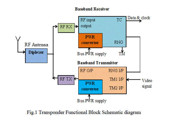
The Baseband subsystem acts as the interface between the satellite and dedicated ground stations. The S-band TT&C (Tracking Telemetry and Command) Transponder consists of all elements for RF reception, demodulation, modulation and RF transmission. In the fig 1, it shows the functional description of the transponder needs to cater to the following functions:
1. The Tele command function, i.e. reception and decoding command signal transmitted from the ground in the specified frequencies.
2. The Telemetry function, i.e. modulation and transmission to ground in specified frequencies.
3. The Ranging function is usedto permit accurate satellite range measurements.
A Transponder is defined to comprise of one Receiver and one Transmitter. Uplinked command signal is demodulated to data level by the receiver. The demodulation is carried at both RF and sub-carrier level. Also the receiver shall demodulate the up-linked ranging signals to video level. The receiver shall accept the DC power (spacecraft bus) input and generate the necessary regulated secondary voltages and shall contain the necessary power interface module.
The receiver shall be powered “ON” with no relay or switch in the DC path. The Transmitter shall linearly phase modulate the Telemetry sub-carriers and ranging signals on a single RF carrier and generate the requisite RF power before transmission. The Transmitter shall accept the DC power (spacecraft bus) input and generate the necessary regulated secondary voltages and shall contain the necessary power interface module. The transmitter shall be powered with ON/OFF provision.
IV.PROPOSED SYSTEM
Modulation and demodulation techniques are used to resist the environmental degradation factors that occur during transmission in the Baseband subsystem. Modulation is the process by which message signal is combined with a high frequency carrier signal in baseband transmitter. The combined signal is at a higher frequency, and less susceptible to degradation when relayed over the transmitting antenna. The demodulation is reverse process, where the high frequency transmitted signal is relayed from the receiving antenna and is down converted to the frequency of the original data in the baseband receiver.
A. BPSK Modulator
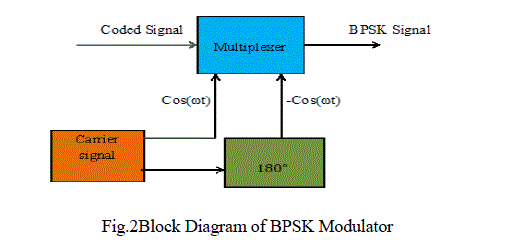
In Baseband Transmitter, the BPSK modulation is used. The input (video signal) is given to the Baseband transmitter. The Coded signal here is NRZ-S (Non Return Zero-Space). After that BPSK modulation process is done.In the transmitter of a communications carrier system, a carrier wave is modulated by a baseband. BPSK refers to the technique of modifying the carrier phase of a signal both before transmission and after receipt. Although there are numerous techniques that could have been utilized to transmit and receive the data, BPSK was chosen for its simplicity and robustness [2], [5].
In the fig 2, it shows the key identifying characteristic of BPSK is that the modulation process creates two separate high frequency carriers depending on the data that is being transmitted, representing either a one or a zero. Binary data are represented by two signals with different phases in BPSK [7]. Typically these two phases are 0 and π, the signals are
s0 (t) = Acos (ωt) 0 ≤ t ≤ T, for 1 (1)
s1 (t) = -Acos (ωt) 0 ≤ t ≤ T, for 0 (2)
Where,
„AâÃâ¬ÃŸ = represents the peak value of sinusoidal carrier.
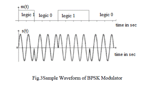
The output of the Baseband transmitter is intermediate frequency (IF) and finally passes to the RF Transmitter. This RF Transmitter passes the signal to Diplexer and it goes to the RF antenna.Baseband refers to the band of frequencies occupied by the information signals before they are used to modulate the RF carrier.in the fig 3;it shows the basic BPSK modulator waveform.
B. BPSK Demodulator
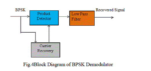
In the Baseband Receiver, IF (intermediate frequency) frequency is converts to the NRZ-L (Non Return Zero-Level) and BPSK demodulation is used. The coherent demodulator of BPSK falls in the class of coherent detectors for binary signals. The coherent detector could be in the form of a correlator. The correlator reference signal is the difference signal
Sd (t) = 2Acos(ωt) (3)
Where the reference signal is the scaled-down version of the difference signal. The reference signal must be synchronous to the received signal in frequency and phase.In the fig 4, the carrier is recovered by the carrier recovery circuit. The BPSK modulated signal is multiplied with the sine wave generated by the carrier recovery circuit.
Keywords
BPSK, FPGA, Xilinx, Baseband, Transponder, VHDL
I.INTRODUCTION
A digital modulation system is more reliable than analog modulation. The main aim of the paper is to create a BPSK (Binary Phase Shift Keying) modulation and demodulation using Xilinx ISE software in digital baseband subsystem. Binary Phase Shift Keying (BPSK) modulation is widely used modulation scheme in telemetry chain of satellites due to its power efficiency. The modulation scheme employed for telemetry transmission is PCM/BPSK/PM [1]. The BPSK is done at S-band frequencies (2-4) GHz, the BPSK subcarriers are basically at 32 KHz and 128 KHz. The digital modulation technique can be said to be the unpretentious form of phase modulation and is identified as binary because the carrier phase epitomizes only two phase 0âÃÂðand 180°. It is habitually used for high speed data transfer application, and is forceful and simple in the implementation [2].
Digital modulator is the method by which digital symbols are transmitted into waveforms that are suited with the appearances of the channel. The BPSK modulation technique is humblest and most vigorous of all PSK modulation techniques since it takes the highest level of noise or distortion to make the demodulator reach an incorrect decision. It is, however, only able to modulate at 1 bit/symbol and so is unsuitable for high data-rate applications [2], [3], [4], [7].In BPSK modulation the phase of the carrier signal is varied according to the modulating signal. In BPSK modulation the output of logic 0 is phase shifted at lower level and logic 1 is phase shifted at upper level [3]. Depending on the logical condition of the digital input, the carrier is transferred to the output, either in phase or at 180° out of phase, with the reference carrier oscillator. The input signal to the multiplexer can be +cos (ωt) or –cos (ωt).The major advantages of using digital modulation technique are that the use of digital signals diminishes hardware, noise and interference hitches as compared to the analog signal. In Baseband Subsystem BPSK modulation and demodulationused for transmitting and Receiving the signal.
II.RELATED WORK
Anshuman Sharma et al.deliberates that the BPSK demodulator were executed on ALTERA platform. The BPSK demodulator in this work is programmability but the higher clock requirement of 32.256 MHz can still be further enhanced to a lower clock if the FIR filter i.e. Kaiser filter in the demodulator front end is implemented with further parallelism and also the bit synchronizer is prepared to work with precisely two samples per bit [1].
Shruti Helonde et al. had implemented the BPSK modulator in Simulink it has two sine wave generator, a binary data source and a switch. According to the second input, first and third input is controlled. If the second input is logic 0 then sine wave is the output of the switch and if the input is logic1 then output is 180 degrees phase shifted sine wave. The modulated signal added with noise arrives at the input to the BPSK Demodulator [2].
Pratik. A et al. confers the BPSK System implemented on the Spartan 3E Starter Kit board has the same principle as the implementation in System Generator. Although System Generator has an option to generate the VHDL code, for this design the code was made from the beginning because the generated code was hard to read. The only difference was that of the carrier which was indeed generated internal, in a ROM memory, but made of 16 different values. The yielded carrier with 180º phase shift was obtained by reading the ROM memory later with 8 samples. If the input signal is within the limits of upper and lower bounds, the input signal passes through unchanged, otherwise signal is clipped to the upper and/ or lower bounds[3].
Hina Malik et al. had implemented the BPSK modulatorand demodulator by using hardware description language (VHDL) and implementing it on Spartan 3E FPGA kit. Both, the modulating signal and the carrier are generated internally the modulating signal by a LFSR and the carrier by a DDS Compiler. The modulated signal is obtained at the output of a mux block and then, passed through a communication channel where noise is added [5].
Thotamesetty et al. had implemented the BPSK modulator in two different ways. First, with simple block and second, with a block in MATLAB code.Then, we made a proposal of three implementations of a BPSK modulator in System Generator. In the first, the three signals: the carrier, the modulating and the modulated signals where generated external. In the second scheme, the carrier is generated external, and the modulating signal is generated internal by a LFSR. And in the third scheme, all three signals were generated internal with the exception of the modulating signal which can be obtained either internal by the LFSR, or external by the pulse generator. By using system generator further the carrier signal is generated internal by DDSblocks and the modulating signal can be generated internal by the LFSR and externalby the Agilent 81101A Pulse Generator [6].
III.SYSTEM ARCHITECTURE
The Baseband subsystem acts as the interface between the satellite and dedicated ground stations. The S-band TT&C (Tracking Telemetry and Command) Transponder consists of all elements for RF reception, demodulation, modulation and RF transmission. In the fig 1, it shows the functional description of the transponder needs to cater to the following functions:
1. The Tele command function, i.e. reception and decoding command signal transmitted from the ground in the specified frequencies.
2. The Telemetry function, i.e. modulation and transmission to ground in specified frequencies.
3. The Ranging function is usedto permit accurate satellite range measurements.
A Transponder is defined to comprise of one Receiver and one Transmitter. Uplinked command signal is demodulated to data level by the receiver. The demodulation is carried at both RF and sub-carrier level. Also the receiver shall demodulate the up-linked ranging signals to video level. The receiver shall accept the DC power (spacecraft bus) input and generate the necessary regulated secondary voltages and shall contain the necessary power interface module.
The receiver shall be powered “ON” with no relay or switch in the DC path. The Transmitter shall linearly phase modulate the Telemetry sub-carriers and ranging signals on a single RF carrier and generate the requisite RF power before transmission. The Transmitter shall accept the DC power (spacecraft bus) input and generate the necessary regulated secondary voltages and shall contain the necessary power interface module. The transmitter shall be powered with ON/OFF provision.
IV.PROPOSED SYSTEM
Modulation and demodulation techniques are used to resist the environmental degradation factors that occur during transmission in the Baseband subsystem. Modulation is the process by which message signal is combined with a high frequency carrier signal in baseband transmitter. The combined signal is at a higher frequency, and less susceptible to degradation when relayed over the transmitting antenna. The demodulation is reverse process, where the high frequency transmitted signal is relayed from the receiving antenna and is down converted to the frequency of the original data in the baseband receiver.
A. BPSK Modulator
In Baseband Transmitter, the BPSK modulation is used. The input (video signal) is given to the Baseband transmitter. The Coded signal here is NRZ-S (Non Return Zero-Space). After that BPSK modulation process is done.In the transmitter of a communications carrier system, a carrier wave is modulated by a baseband. BPSK refers to the technique of modifying the carrier phase of a signal both before transmission and after receipt. Although there are numerous techniques that could have been utilized to transmit and receive the data, BPSK was chosen for its simplicity and robustness [2], [5].
In the fig 2, it shows the key identifying characteristic of BPSK is that the modulation process creates two separate high frequency carriers depending on the data that is being transmitted, representing either a one or a zero. Binary data are represented by two signals with different phases in BPSK [7]. Typically these two phases are 0 and π, the signals are
s0 (t) = Acos (ωt) 0 ≤ t ≤ T, for 1 (1)
s1 (t) = -Acos (ωt) 0 ≤ t ≤ T, for 0 (2)
Where,
„AâÃâ¬ÃŸ = represents the peak value of sinusoidal carrier.
The output of the Baseband transmitter is intermediate frequency (IF) and finally passes to the RF Transmitter. This RF Transmitter passes the signal to Diplexer and it goes to the RF antenna.Baseband refers to the band of frequencies occupied by the information signals before they are used to modulate the RF carrier.in the fig 3;it shows the basic BPSK modulator waveform.
B. BPSK Demodulator
In the Baseband Receiver, IF (intermediate frequency) frequency is converts to the NRZ-L (Non Return Zero-Level) and BPSK demodulation is used. The coherent demodulator of BPSK falls in the class of coherent detectors for binary signals. The coherent detector could be in the form of a correlator. The correlator reference signal is the difference signal
Sd (t) = 2Acos(ωt) (3)
Where the reference signal is the scaled-down version of the difference signal. The reference signal must be synchronous to the received signal in frequency and phase.In the fig 4, the carrier is recovered by the carrier recovery circuit. The BPSK modulated signal is multiplied with the sine wave generated by the carrier recovery circuit.
V. RESULT AND DISCUSSION
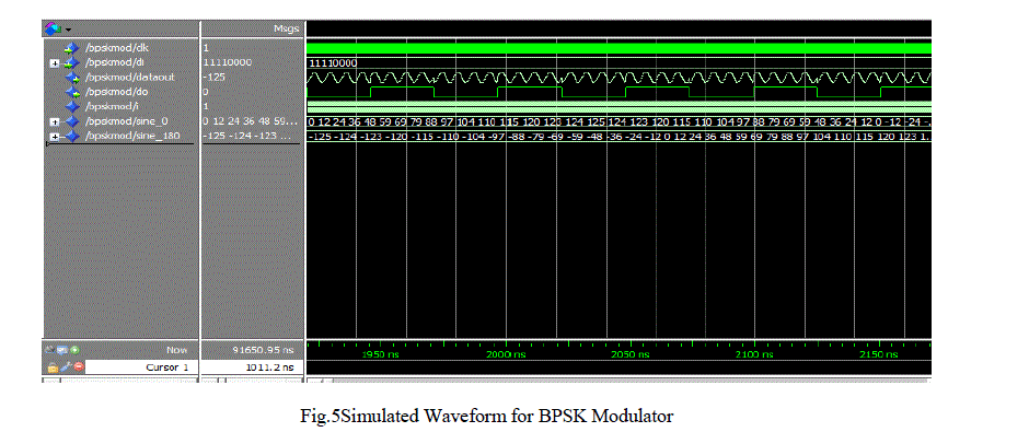
After performing the above steps, the program is run with the inputs of IF is 16 KHz for the Baseband Receiver are given by the user and video signal are taken from the spacecraft will perform in the Baseband Transmitter. The digital domain compared to the analog domain provides manifold benefits like easy calibration, higher accuracy and better predictability. In the fig 5, it shows the BPSK modulator waveform in Baseband Transmitter.
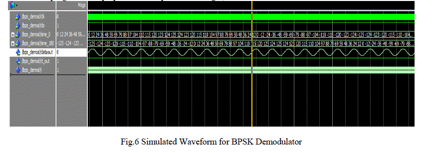
As per the analysis of time, processing of the proposed system has improved the high accuracy. In the Baseband transmitter,the video signal are engaged as input and prearranged to the NRZ-S and the BPSK modulation progression is prepared in the downlink. In the Baseband receiver,the IF frequency are renovate to the NRZ-L and the BPSK demodulation progression is prepared in the uplink. In the fig 6,it shows the BPSK Demodulator waveform.
VI.CONCLUSION
In this work, we have built a simulation model to analyze the BPSK modulation and demodulation. The BPSK design gives an accurate output without any delay. Future work will focus toimplement the BPSK Modulation and Demodulation on FPGA kit. The main advantage of selecting FPGA is to provide a larger number of input/output ports and the parallel implementation of hardware results in faster algorithm execution.
VII.ACKNOWLEDGEMENT
The authors sincerely acknowledge SAMEER-CEM for allowing to doing the project. The authors would like to thank Mrs G. Kalaichelvi and L. Mohan, Digital Signal Processing Division for their valuable inputs. The authors would like to thank all the volunteers for their time and effort to make this study possible.
References
Anshuman Sharma, Abdul Hafeez Syed, Midhun M, MR Raghavendra, “Realization of Programmable BPSK Demodulator-Bit Synchronizer using Multirate Processing,”International Journal of Electrical and Computer Engineering,Vol. 4, No. 3, pp. 433~440, June 2014.
Shruti Helonde, M. S. Pawar, “BPSK Modulation Technique forDigital Communication,” E-ICETT 2014.
Pratik A. Bhore, Mamta Sarde, “BPSK Modulation and Demodulation Scheme on Spartan-3 FPGA,” IORD Journal of Science & Technology, Volume 1, Issue III, PP 38-45, MAR-APR 2014.
S.O. Popescu, A.S.Gontean and G.Budura, “BPSK System on Spartan 3E FPGA,” SAMI 2012, 10th IEEE Jubilee International Symposium on Applied Machine Intelligence and Informatics, January 2012.
Hina Malik, D.R.Rotake , Mamta Mahajan,“Design and Implementation of BPSK Modulator and Demodulator Using VHDL ,”IOSR Journal of Electronics and Communication Engineering, Volume 9, Issue 3, Ver. IV,PP 98-105,May - Jun. 2014.
Thotamesetty M Prasad, Syed jahingir, “Simulation and implementation of a BPSK modulator on FPGA,”International Conference on Electronics and Communication Engineering, 16th September 2012.
Bhosle S. S., S. A. Shirsat, A. D. Jadhav, “Hardware Simulation of BPSK Modem,”International Journal of Computer Applications (0975– 8887) International Conference and Workshop on Emerging Trends in Technology 2013.
J.G. Proakis, Digital Communications, 5th edition, McGraw Hill New York, 2001.
J.S.Ruque, D.I.Ruiz, C.E. Carrion, “Simulation and implementation of the BPSK modulation on a FPGA,” IEEE Transactions on Education, Vol.48, No.1,2011.