International Journal of Advanced Research in Electrical, Electronics and Instrumentation Engineering
ISSN ONLINE(2278-8875) PRINT (2320-3765)
ISSN ONLINE(2278-8875) PRINT (2320-3765)
| S.Sujatha1, M.Vignesh2, V.Govindaraj3 |
| Related article at Pubmed, Scholar Google |
Visit for more related articles at International Journal of Advanced Research in Electrical, Electronics and Instrumentation Engineering
A low power dual edge triggered flip flop based on a signal feed through scheme is presented. The power consumption is the major problem in circuit design. The proposed deign reduces power and delay compared to explicit pulse triggered flip flop. Reducing the number of transistor in the stack and increasing the number of charge path leads to higher operational speed compared to others flip-flops. Double-edge-triggered flip flops (DETFFs) are recognized as power-saving flip flops. The dual edge triggered design operates in a low voltage range and hence it is suited for low voltage application. This flip flop uses weak feedback transistor but without static power consumption. This reduces leakage current and thus saves the power. By using low clock frequency high throughput can be achieved. The simulation is done using Tanner EDA Tool v14 with CMOS 90nm technology.
Keywords |
| Flip Flop, Low Power, Delay, Dual Edge, Area |
INTRODUCTION |
| The dynamic power consumption in the clock tree depends on the frequency and the load of clock tree. If the sampling of the input is performed in both rising and falling edge of clock (Double-Edge triggered) [3], the frequency of the clock can be half of the clock frequency of the single edge triggered FF called Double-edge triggered Flip-Flop. Double-edge triggered Flip-Flop (DETFF) has less dynamic power consumption, static power, and delay compared to the previous flip-flops. Dual edge-triggered flip flops are becoming a popular technique for low-power designs since they need halving of the clock frequency. A double edge-triggered flip flop can be designed by two transparent latches in parallel whereas single-edge triggered flip flop in series. Dual-edge triggered flip-flop passes data at both positive as well as negative edges of the clock. |
| This supports many applications where the throughput is very high. Flip-Flops are important storage elements in digital circuits that play a major role on circuit power consumption and speed. An alternative clocking approach is the use of dual edge triggered flip flop which captures data on both rising and falling edges of the clock. Same data throughput can be achieved at half of the clock frequency as compared to single edge triggered Flip-Flops. We can say that double edge clocking can be used to save half of the power in the clock distribution network. Dynamic or switching power dissipation and leakage power depends on supply voltage. Since Dynamic power is proportional to the square of the supply voltage it is the highest power consumption among the three. Hence the major step to be taken is to reduce the dynamic power. By reducing the supply voltage dynamic power can be reduced. This may affect the speed of the circuit. Reduction in clock frequency is another alternative to reduce the dynamic power. By using Double edge clocking, clock frequency can be reduced. In this approach same data throughput can be achieved with half of the clock frequency as compared to SETFF [4]. Single edge triggered flip flop takes many cycles to pass the data whereas dual edge triggered flip flop takes only few cycles to sample the data. |
II. RELATED WORK |
| The low power and area plays a significant role in the circuit design. In order to reduce that dual edge triggered flip flop is discussed. Here conditional capture, conditional precharge, conditional discharge, and conditional pulse enhancement scheme techniques [2] are discussed. They suffer from longer discharging path hence the data transition takes more time. In pulse triggered flip flop signal feed through scheme is adopted by using pass transistor. In order to reduce power and area, dual edge triggered flip flop is used. As for the Differential class, two topologies emerge as the most energy-efficient ones: DET-SPL (Static Pulsed Latch) in the high speed region and the DET-TGLM in the low-energy on. In particular, DET-TGLM (Transmission Gate Latch MUX) dissipates less energy among all the analyzed FFs. This is due to the combination of the DET and MS features, which both contribute to reduce energy consumption. The DET functionality is simply accomplished by adopting a DET Pulse Generator. DET-CDFF has an EP structure and shows a good tradeoff but is competitive only for the FOM. DET-SPGFF, which is an implicit pulsed FF, is never the most energy-efficient FF because it suffers from a high layout complexity, and also from the inclusion in the paths of the clocked precharge transistors, which thus need to be oversized. MS FFs are clearly the most energy-efficient FFs in the low energy region, whereas their speed is limited. Together with TGPL, TGFF, and DET-TGLM offer also the best compromise in terms of product. Clock-gated FFs are by far the worst circuits and have a degraded speed and energy compared to any other topology. Accordingly, Clock-gated FFs are unsuitable for nanometer technologies. Among [3] DET FFs, the DET-TGLM represents the most energy- efficient solution in the deep low-energy region, together with TGFF. It is the DET counterpart of TGFF and they show similar performances since the greater layout complexity of DET-TGLM is compensated by the energy reduction due to the DET property. |
III. EXISTING DESIGNS |
| The pulse generation can be classified into implicit and explicit type. Implicit type does not occupy much space and is inbuilt within the circuit, no external signals are needed. Power consumption is less in implicit type but it suffers from longer discharging path. In explicit type pulse generator and latches are separate. Hence the power consumption is more. Thus to reduce the power consumption and circuit complexity a single pulse generator can be shared by a group of FFs. Here explicit type designs are discussed. Some existing flip flops are compared here. |
A. CONVENTIONAL EXPLICIT TYPE P-FF DESIGNS |
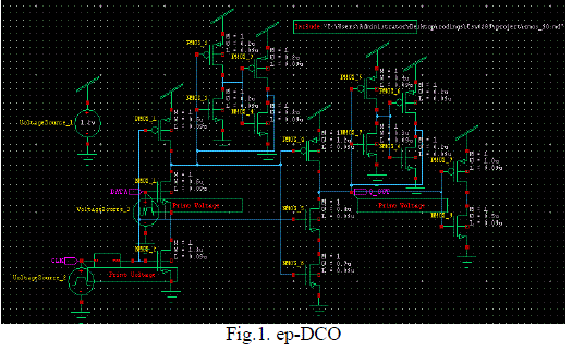
| Fig.1. shows a classic explicit type data close to output. It contains a NAND-logic-based pulse generator and a semi dynamic true-single-phase-clock (TSPC). In this P-FF design, inverters I3 and I4 are used to store data, and inverters I1 and I2 holds the internal node X. The delay of three inverters determines their pulse width. A drawback here is even if their static input is 1 the internal node X is discharged on every rising edge of the clock. Some techniques are used to overcome this problem. They are conditional capture, conditional precharge, conditional discharge, and conditional pulse enhancement scheme [2]. |
 |
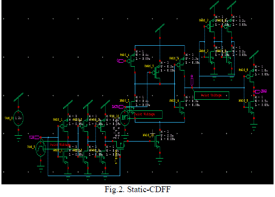
| Fig.2. shows the static conditional discharge technique. It has longer data to Q delay compared to CDFF. Since three stacked transistor is used it faces worst case delay [3]. To overcome this delay a pull down circuitry is used but the disadvantage is that extra layout area and power consumption. |
 |
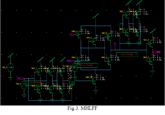
| The modified hybrid latch flip flop (MHLFF) shown in Fig.3. The keeper logic at node X is removed. This is satisfied by having a weak pull-up transistor MP1controlled by the output signal. Thus Q maintains the level of node X when Q equals 0. There are two drawbacks in the MHLFF design. First, a prolonged 0 to 1 delay is expected. Second, node X becomes floating sometimes and its value may drift causing extra dc power |
 |
B.PULSE TRIGGERED FLIPFLOP |
| The pulse triggered flip flop with signal feed through scheme [1] is mainly used to reduce the delay when the data transition occurs. The signal feed through scheme is composed of pass transistor.Fig.4. Shows the pulse triggered flip flop. |
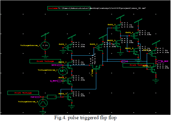 |
| This design has three major difference compared to other circuits. |
| ïÃâ÷ First the weak pull up PMOS transistor is grounded. Here pseudo NMOS logic style is followed thus the internal node X is saved |
| ïÃâ÷ Second a pass transistor is used to feed the input directly. The pass transistor is controlled by clock and thus reduces delay during transition of data. By using signal feed through scheme a boost can be applied directly to the pass transistor and reduces the delay and shortens the data transition. The second stage inverter is removed in this design hence data passes from source to Q immediately. The MNX is used for two purposes mainly providing extra driving to node Q during 0 to 1 data transitions, and discharging node Q during “1” to “0” data transitions .Extra NMOS transistor facilitates signal feed through scheme [1] and thus reduces the switching activity. |
IV.PROPOSED DESIGN |
| The input of the flip-flop is transferred to the output at the rising and falling edges of the clock. Since pass transistor is used the power consumption is minimized [1]. The data is triggered at both the edges simultaneously hence the clock power is reduced. The clock power distribution is major problem hence the above technique is preferred. This design gives high throughput compared to single edge triggering. The frequency needed for dual edge triggering is half the frequency compared to single edge triggering |
| The dual edge triggered flip flop thus leads to higher operating speed by reducing delay. It also reduces area by triggering both positive and negative edges simultaneously. It also reduces sensitivity to pulses noise. |
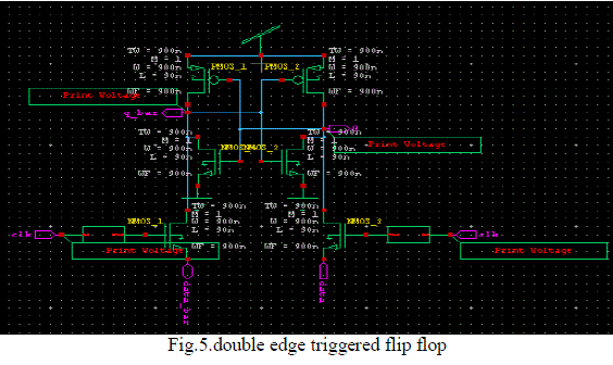 |
| The inverters are used in the dual edge triggered flip flop instead of NAND logic gate. The input is given to the NMOS on both sides and clock is also given. When the input is given, the inverter triggers the data on both rise edge and fall edge. Hence the data transition is faster when the clock is given. The existing design occupies more area because of NAND gate. In proposed design since only inverter is used area is reduced. In Single edge triggered flip flop the data triggers either on positive edge or on negative edge. It takes many cycles to pass the data. For each pulse generator NAND gate is used in existing design. The inverters reduce the discharging path when the data is transmitted from 0 to 1 and from 1 to 0. |
IV. RESULTS AND DISCUSSION |
| The results are obtained by using Tanner EDA Tool v14. This compares the power for various designs of flip flops with the proposed design and thus shows the improvement in power and area. Here the simulation results are obtained for dual edge triggered flip flop along with signal feed through scheme. |
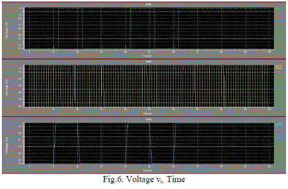 |
| Fig.6. Shows the simulation output waveforms of pulse triggered flip flop. The power consumption and area of pulse triggered flip flop are shown in Table .1. |
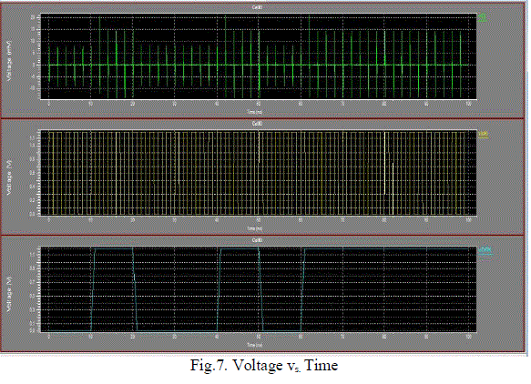 |
| Fig.7. Shows the simulation output waveforms of the dual edge triggered flip flop. The power consumption and area of the dual edge triggered flip flop are shown in Table .1. |
| The comparison table below shows the power consumption and area for various designs. From this table it is clear that the proposed design has the lowest power consumption when compared with other designs. |
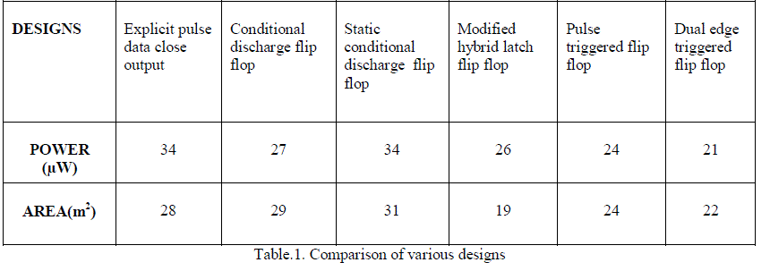 |
| Dual-edge-triggered flip-flops (DETFF's) offer potential advantages with respect to speed and power supply requirements. Since data can be transmitted at both rise edge and fall edge dual edge triggered flip flop consumes low power. It also reduces delay when the input is given. Nearly 40 percent of the power consumption can be saved. Already the pass transistor is used to enhance the signal feed through directly in order to reduce power. In addition to that dual edge triggered flip flop is used in the design to save the power. |
References |
|