International Journal of Advanced Research in Electrical, Electronics and Instrumentation Engineering
ISSN ONLINE(2278-8875) PRINT (2320-3765)
ISSN ONLINE(2278-8875) PRINT (2320-3765)
| Gagandeep Singh1, Mandeep Singh Angurana2 |
| Related article at Pubmed, Scholar Google |
Visit for more related articles at International Journal of Advanced Research in Electrical, Electronics and Instrumentation Engineering
A three stage Voltage Controlled Ring Oscillator (VCRO) has been designed, analysis and simulated in 50 nm CMOS Technology by using LT spice. The designed circuit proposed a wide tuning range of operating frequency with very low of supply voltage and low power consumption that can be used for various applications. The designed circuit is operated at 0.8 V to 1.2 V supply Voltage to obtain wide operating frequency range which simulated results show range of about 10 GHz with minimum frequency of 0.80 GHz to 11.64 GHz. The designed circuit provides minimum power consumption of 4.45μW.
KEYWORDS |
| Voltage Controlled ring oscillator (VCO), wide tuning range, low supply voltage, power consumption and phase noise |
INTRODUCTION |
| After explosive growth in the last decade the oscillators becomes a most commonly used component in any modern semiconductor IC system used for communication, clock recovery circuits, microprocessors and phase locked loops and also used in the digital electronic circuits to provide a reference clock signal. The VCO has many useful applications some are like used as impulse based ultra wideband transmitter for biomedical applications, for GPS/Galileo applications, for spectrum Monitor receiver in Cognitive Radio Applications, for non contact vital sign radar applications, communication industry, wireless sensor network applications, IMT advanced and UWB applications. In today’s communication system, a VCO with high operating frequency, low power consumption, low phase noise is first and foremost requirement. To obtain optimized values of VCO has been one of the motivations behind this work. As compare to LC VCO, the ring voltage controlled oscillators are more reliable and suitable for the wide tuning range and consume extremely less area than inductor and varactor. On the other hand LC resonant VCO exhibits better phase noise with having high quality factor than ring oscillators but due to inductor flow complexity, cost and chip area is increases. The ring oscillator provides much better wide tuning range as trade of phase noise. Different designs are proposed by many analog designers and further research is going on this topic. The architecture proposed in [7] is less power efficient due to lack of PMOS diode pair to perfectly cancel out the resistive load. The design proposed in [8] frequency is tuned by Vgs of PMOS cross coupled load which results in limited tuning range. The delay cell proposed in [3] provides better tuning range but the power consumption is not much effective. The delay cell proposed by Panigrahi and Acharya [1] provide wide frequency tuning range with low power consumption is considered for analysis in this work. The work reported in [1] uses 90nm CMOS technology and hence needs performance evaluation when 50nm CMOS technology is used for circuit design. This has been one of the motivations behind the current work. |
| In this paper a three stage CMOS differential voltage controlled ring oscillator using 50nm technology is analyzed and compared with the various previous designed. This paper is organized as follow. In section II the analysis of VCO ring oscillator circuit block diagram and design is discussed. Section III the presents the simulated waveforms, tuning range, power consumption and phase noise is discussed. At the end of this paper a comparative study of other oscillators and technology is taken out. |
II. VCO CIRCUIT DESIGN |
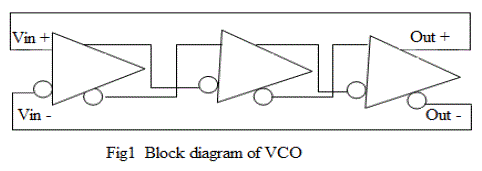
| The double ended differential ring oscillators are very less prone to noise and irregularities as compare to the single ended voltage control oscillator with the trade off of achieve higher frequency range. In differential ring oscillators phase noise can be improved by increase the number of stages of ring oscillator. The block diagram of three stage differential ring oscillator is shown in figure 1. |
 |
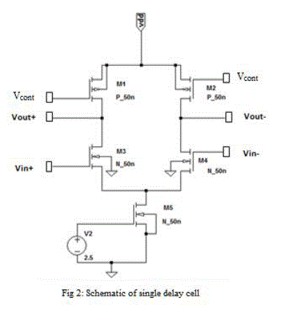
| The Schematic of delay cell analysed in this paper is shown in figure 2. The schematic of delay cell includes M1 and M2 are two PMOS transistor operate from deep triode region to saturation region, whose gate to source voltage is varied to get the desired output frequency of oscillation, M3 and M4 are two NMOS transistor with input voltage operating in a saturation region, M5 is the NMOS transistor used to provide a constant current source i.e. act as constant current source operate in a saturation region. Here M1 and M2 operate in the triode region thus each transistor acting as a variable resistor controlled by Vcont. As the Vcont become more positive the resistance of M1and M2 transistor increases, thus raising the time constant at the output and lowering the operating frequency at the output. |
 |
III. WIDE TUNING RANGE |
| The oscillation frequency of N-stage ring oscillator can be expressed as |
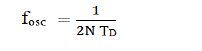 |
| Where N is the number of stages of ring oscillator, fosc frequency of output waveform and TD is the delay of the each stage in ring oscillator i.e. to vary the frequency TD can be adjusted. As the Vcont becomes more positive the resistance of M3 and M4 increases, thus raising the time constant at the output lowering the fosc. |
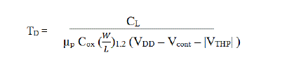 |
| The frequency of oscillation can be expressed as |
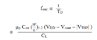 |
| Where CL is the total capacitance seen at each output to ground, (W/L) is the aspect ratio of M1 and M2 PMOS transistor 1μm/50nm, VTHP is the threshold voltage of PMOS |
IV. POWER DISSIPATION |
| The differential ring oscillator produce low power dissipation as compared to the LC voltage controlled oscillator due to the NMOS input pair (M3 and M4) used to maximize the transconductance to capacitance ratio (gm/c) to achieve high operating frequency with low power dissipation. In order to reduce the gm requirement and thus power dissipation, only parasitic capacitors of devices are utilized. |
V. SIMULATION RESULTS AND DISCUSSION |
| The differential ring oscillator is designed and simulated in LT spice tool. The tuning range, power dissipation parameters are analysed and compare with the other designs. |
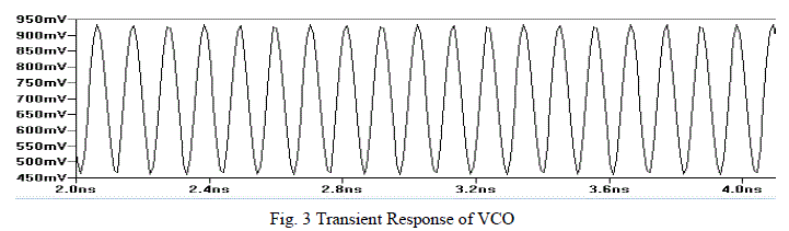 |
| In the fig 3, it shows the transient response of VCO at VDD = 1V and VCont =0.5v with 2.5 v across the gate to source terminal of M5 NMOS transistor to work as a current source, providing a frequency of about 8 GHz. |
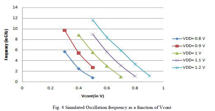 |
| In the fig 4, it shows the graph of different operating frequency which is obtained by varying the supply voltage from range of 0.8V to 1.2 V and varying the VCONT (voltage across the gate and source terminal of M1 and M2 PMOS transistor) at different voltage supply. |
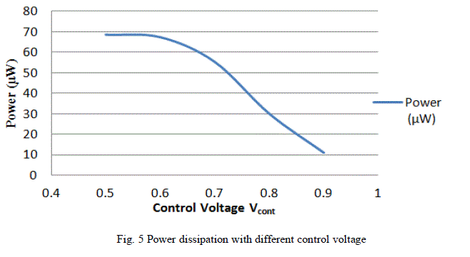 |
| In the fig 5, it shows the graph of power dissipation of VCO varies with different power supply due to maximize the output swing, the source terminal of M1 and M2 transistors are directly connected to power supply. The maximum power dissipation is 68.66 μW when supply voltage is 1.2 V and Vcont is 0.5V and minimum dissipation is 4.40 μW when supply voltage is 0.8 and control voltage is 0.5V. |
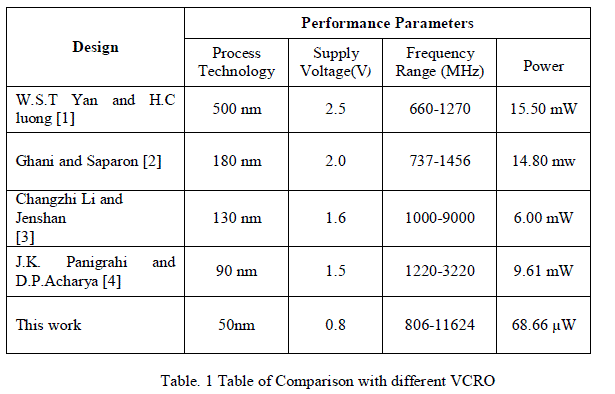
VI. COMPARISION OF RESULT |
| Various designs are designed with different supply voltage and different technologies. A comparison of different design is analysed in Table 1 |
 |
VII. CONCLUSION |
| A wide operating frequency range of 0.8 GHz to 11.64 GHz is determined with the tuning range of about 10 GHz, which is wider than other designs. Power consumption is of about 4.32 μW at 0.8 V supply voltage and 68.66 μW at 1.2V supply. The proposed design can be used for various electronic welfares. |
References |
|