International Journal of Advanced Research in Electrical, Electronics and Instrumentation Engineering
ISSN ONLINE(2278-8875) PRINT (2320-3765)
ISSN ONLINE(2278-8875) PRINT (2320-3765)
Bini.D1, Janani.J2, Nandhini.J2 and Anusooya.S3
|
| Related article at Pubmed, Scholar Google |
Visit for more related articles at International Journal of Advanced Research in Electrical, Electronics and Instrumentation Engineering
This design describes a high resolution Digital Voltmeter embedded design in a single PSoC chip, which can measure wide range of voltages between 1millivolts – 5volts and found suitability in sensor applications. This design is implemented in a PSoC3 device IC CY8C3866. The design implements analog and digital user modules: a buffer, 20 bit ADC, UART and LCD. The ADC gets the analog input from measurement signal or from sensors and the digitized output is sent to serial port through UART module. User friendly menu driven program written in LABVIEW acquires the serial data from PSoC chip and the acquired measurement data is displayed on the PC menu screen as well as saved in a user specified file path. The user interacts only with the graphical screen designed for the project; hence PC is used only as an input-output device.
Keywords |
| PSoC, LABVIEW, Virtual Instrument. |
INTRODUCTION |
| Digital Voltmeters are generally designed with an analog-to-digital Converter called an integrating converter. In any measurement devices, resolution is a one of the very important specification. Resolution is the smallest change in an input signal for a noise free voltmeter which produces on average, a change in the output signal. Resolution of DVM can be expressed in bits, absolute units or digits. In this design high resolution analog system has been implemented using an integrated, highly configurable, 20-bit Delta-Sigma ADC in a PSoC internal. |
| PSoC based DVM integrate the buffer, ADC, UART and LCD in a single chip. Both analog and digital components can be configured and reconfigured for any required task in the embedded applications. The digitized analog data from the ADC is sent through UART to serial port. The output of PSoC is read by the user friendly menu driven program developed in LabVIEW, a graphical language. The measured data is displayed in the graphical user interface (GUI) front panel. The values are plotted on-line as well as saved in a user specified file path. |
| This design is unique in such a way the required analog and digital modules for the entire functionality are programmed on a single chip. The analog, digital and digital communication blocks are integrated in the microcontroller. The PSoC allows creating peripheral functions which are customized to match the requirement for any specific application and provide cost effective design solution. The menu driven GUI program written in LABVIEW establishes a Virtual Instrument programming concept for the design and also for communicating with PSoC through the serial port of the computer. The benefit of LABVIEW is to produce the graphical programming especially for data acquisition and control measurement thereby providing the required user interface through PC and emulate instruments virtually. |
PROGRAMMABLE SYSTEM ON CHIP |
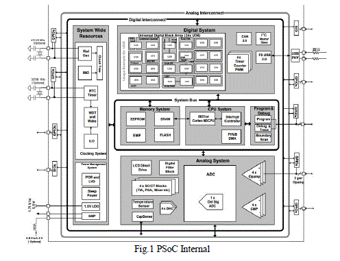
| Programmable System of Chip (PSoC) is software configured, mixed signal array with a built-in MCU core. A PSoC IC has a core, configurable analog and digital blocks and programmable routing and interconnects as shown in fig.1. |
| PSoC3 chip has single cycle 8051 core upto 67 MHz which can be routed to multiple pin location providing flexible routing and eliminate the fixed function pins. PSoC3 architecture boosts performance through integrated high-precision 20-bit resolution analog, ultra-low power with industry’s widest voltage range and programmable logic device (PLD) based logic. |
| PSoC creator is an Integrated Design Environment (IDE) which allows concurrent hardware and application firmware design. The components are represented by an icon that users can drag-and-drop into a design and configure with a component customizer to suit a broad array of application requirements. |
 |
DESIGNING IN PSoC CREATOR |
| Cypress’s PSoC creator is easy-to-use second generation software Integrated Development Environment (IDE) that combines a hardware and software design environment based on classic schematic entry and revolutionary embedded design methodology [8]. |
| In this project IC CY8C3866 device was used as the basic platform. PSoC Creator 2.2, an Integrated Development Environment (IDE), is the design tool used for designing and debugging this design application. Cypress JTAG programmer is used for programming the PSoC3 board. |
| Design flow has 4 steps |
 |
| A. Configure |
| In the confirmation step, the peripherals are chosen from a catalog of pre-tested and pre-defined component. Configuration is made by drag and drop method. |
| B. Develop |
| PSoC combine C Based development flow with automatically generated software Application Peripheral Interface (API) for the component in the device. Simple and fast controlling of On-Chip peripherals is done using API. It also reduces coding error and ensures correct interaction with peripherals and makes the whole software development less error prone. |
| C. Debug |
| The state of internal conditions and its functions of an on-chip component are known by debugging the PSoC creator. It shows the type, address and value of variable and has the ability to set breakpoint in code. Most importantly, this mode shows the execution flow of the program |
| D. Reuse |
| The encapsulation of a working design into a reusable component makes it quick and easy to create future design with few errors and less cluttered schematic. |
LABVIEW |
| Laboratory Virtual Instrumentation Engineering Workbench is a platform and development environment for a visual programming language from National Instruments. LABVIEW can be operated on a variety of platforms including Microsoft windows for data acquisition, instrument control and industrial automation [5]. |
| Each Virtual Instrument has a block diagram, a front panel and a connector panel. Front panel allow an operator to input data into or extract data from a running virtual instrument and also serves as program interface. |
EXPERIMENTAL SETUP |
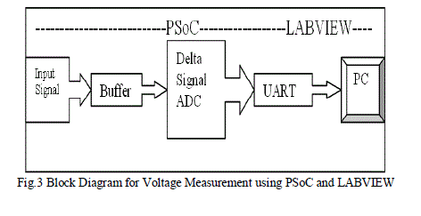
| The basic voltmeter measurement circuit block diagram shown in fig. 3 uses a delta sigma analog to digital converter, provides a low power, low noise front end for precision measurement applications. The circuit consists of a buffer, a 20-bit delta sigma ADC and an UART. The ADC is configured in differential mode and the conversion rate, reference voltage, input modes are selected in the global resource table of PSoC creator tool. |
| The ADC gets the input from the measurement or from sensor and the digitized output is sent through UART to serial port. The measured data is displayed in the menu driven screen of LABVIEW and also saved in a user specified file path. |
 |
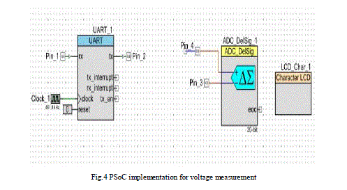
PSoC IMPLEMENTATION FOR VOLTAGE MEASUREMENT |
| The placeable user modules used in the design are 20-bit ADC, UART and LCD. The input signal are fed to ADC which are configured for measuring voltage in a wider range of 1 milli volts to – 5000 milli volts. |
 |
LABVIEW IMPLEMENTATION FOR VOLTAGE MEASUREMENT |
| In this design, LABVIEW has been used for giving a graphical user interface and also for communicating with PSoC through the serial port of the computer as shown in fig. 5. The measured data is displayed in the menu screen as well as saved in a user specified file path. |
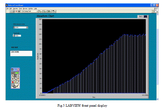 |
| In Fig.3, the waveform chart displays the Time(s) Vs Amplitude (millivolts). |
RESULT |
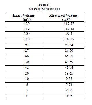
| The table 1 shows the measured voltage values using this PSoC embedded design. |
 |
CONCLUSION |
| A high resolution digital voltmeter designed and implemented for measuring voltages in the wider dynamic ranges. By configuring 20-bit ADC, a 5½ digit DVM has been designed for measuring voltage in the range of 5000 milli- volts-1 milli volt with the resolution of 0.001 mV. |
References |
|