This paper presents the basics of quantum dot cellular automata along with the QCA logic devices such as the QCA wire, inverter and the majority gate. The four phases of the clocking have been discussed and also the implementations of the complex gate have been done using the QCADesigner tool. The logical structures such as AND and OR gates using a quantum dot cellular automata 3-input majority gate have been discussed based on which the five-input complex gate have been designed and can be configured into logical structures such as four input AND and OR.
Keywords |
| QCA, majority gate, logic structures, complex gate, QCADesigner. |
INTRODUCTION |
| Current silicon transistor technology faces challenging problems, such as high power consumption and difficulties
in feature size reduction. Nanotechnology is an alternative to these problems. The Quantum dot cellular automata
(QCA) is one of the attractive alternatives [1]. Since QCAs were introduced in 1993 by lent et al, and experimentally
verified in 1997. QCA is expected to achieve high device density, extremely low power consumption and very high
switching speed.QCA structures are constructed as an array of quantum cells with in which every cell has an
electrostatic interaction with its neighboring cells [2]. QCA applies a new form of computation, where polarization
rather than the traditional current, contains the digital information. In this trend, instead of interconnecting wires, the
cells transfer the information throughout the circuit [4]. |
| This paper describes the design of different logical structures in QCA such as AND and OR. These structures are
designed based on the basic logical devices. The paper is organized as follows; the background of QCA technology is
explained in section 2. Section 3, provides the QCA clocking and section 4 describes the QCA Designer tool. Section 5
shows the design and implementation of logical structures in QCA using majority gate. Simulation results follow in
section 6 and conclusions are presented in section 7. |
BACKGROUND |
| A. QCA Basics |
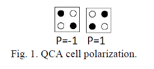
| QCA technology is based on the interaction of bi-stable QCA cells constructed from four quantum dots. The cell is
charged with two free electrons, which are able to tunnel between adjacent dots. These electrons tend to occupy
antipodal sites as a result of their mutual electrostatic repulsion. Thus, there exist two equivalent energetically minimal
arrangements of the two electrons in the QCA cell, as shown in Fig. 1. These two arrangements are denoted as cell
polarization P= +1and P= -1.By using cell polarization P =+1 to represent logic “1” and P = -1 to represent logic “0,”
binary information is encoded in the charge configuration of the QCA cell [2][5]. |
 |
| B. QCA Logic Devices |
| The fundamental QCA logic primitives include a QCA wire, QCA inverter, and QCA majority gate [4]-[6], as
described below. |
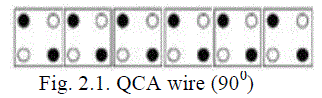
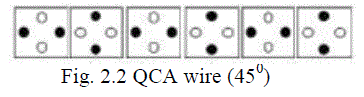
| QCA Wire: In a QCA wire, the binary signal propagates from input to output because of the electrostatic interactions
between cells. The propagation in a 90˚ QCA wire is shown in Fig. 2. Other than the 90˚ QCA wire, a 45˚ QCA wire
can also be used. In this case, the propagation of the binary signal alternates between the two polarizations [4]. |
 |
 |
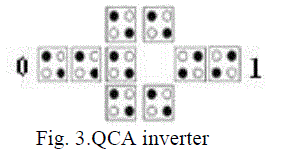
| QCA Inverter: The QCA cells can be used to form the primitive logic gates. The simplest structure is the inverter
shown. Fig. 3, which is usually formed by placing the cells with only their corners touching. The electrostatic
interaction is inverted, because the quantum-dots corresponding to different polarizations are misaligned between the
cells [3]. |
 |
| QCA Majority Gate: The QCA majority gate performs a three-input logic function. A layout of a QCA majority gate is
shown in Fig. 4.1. Assuming the inputs are a, b and c, the logic function of the majority gate is |
| M (a, b, c) = ab+bc+ac. (1) |
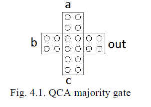 |
| The tendency of the majority device cell to move to a ground state ensures that it takes on the polarization of the
majority of its neighbours. The device cell will tend to follow the majority polarization because it represents the lowest
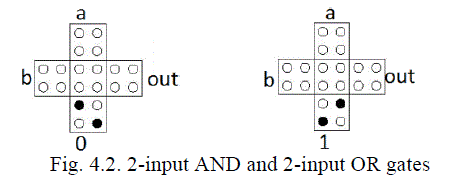
energy state [3]. By fixing the polarization of one input to the QCA majority gate as logic “1” or logic “0” an AND gate
or OR gate will be obtained, respectively, as shown in Fig. 4.2. |
 |
CLOCKING |
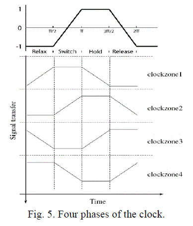
| The QCA circuits require a clock, not only to synchronize and control information flow but also to provide the
power to run the circuit since there is no external source for powering cells. With the use of four phases clocking
scheme in controlling cells, QCA processes and forwards information within cells in an arranged timing scheme. Cells
can be grouped into zones so that the field influencing all the cells in the zones will be the same. A zone cycles through
4 phases. In the Switch phase, the tunneling barriers in a zone are raised. While this occurs, the electrons within the cell
can be influenced by the Columbic charges of neighboring zones. Zones in the Hold phase have a high tunneling
barrier and will not change state, but influence other adjacent. Lastly, the Release and Relax decrease the tunneling
barrier so that the zone will not influence other zones. These zones can be of irregular shape, but their size must be
within certain limits imposed by fabrication and dissipation concerns. Proper placement of these zones is critical to
design efficiency. This clocking method makes the design of QCA different from CMOS circuits. [7]. |
| The Fig. 5. Shows the four available clock signals. Each signal is phase shifted by 90˚ degrees. When the clock
signal is low the cells are latched. When the clock signal is high the cells are relaxed and have no polarization. In between the cells are either latching or relaxing when the clock is decreasing/increasing respectively. |
 |
QCA DESIGNER TOOL |
| QCA logic and circuit designers require a rapid and accurate simulation and design layout tool to determine the
functionality of QCA circuits. QCADesigner gives the designer the ability to quickly layout a QCA design by
providing an extensive set of CAD tools. As well, several simulation engines facilitate rapid and accurate simulation. It
is the first publicly available design and simulation tool for QCA. Developed at the ATIPS Laboratory, at the
University of Calgary, QCADesigner currently supports three different simulation engines, and many of the CAD
features required for complex circuit design. [8],[9]. |
QCA IMPLEMENTATION |
| The AND and OR gates are realized by fixing the polarization to one of the inputs of the majority gate to either P=-
1(logic 0) or P=1(logic 1). |
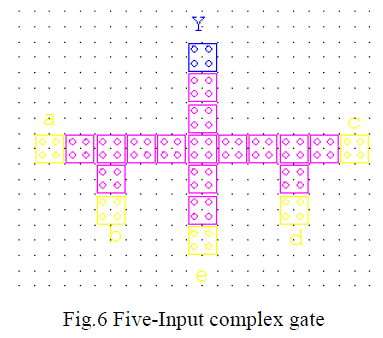
| The same logic is used in the five-input complex gate. This gate is composed of a 3-input majority gate which is
placed in the middle of the complex gate. Here the input „e‟ functions as a control input that is used to specify the
functionality of the circuit. The remaining four inputs a, b, c and d are used to implement logical functions such as
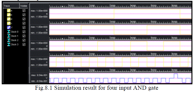
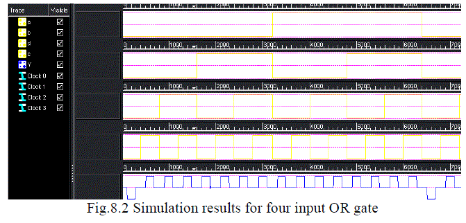
AND and OR. The functionality of this gate for four input AND and OR configurations has been simulated using QCA
Designer. Fig. 6 shows five-input complex gate with a majority gate placed in the middle. |
 |
| A. Four-Input AND Gate |
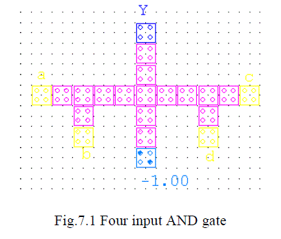
| The five-input gate of Fig. 6 can be used to form a four input AND gate as shown in Fig. 7.1 by restricting input e to
have a fixed polarity that is equal to -1. The selection of „e‟ is unique. For the example circuit as shown in Fig.7.1, the
function represented is Y=abcd. |
 |
| B. Four-Input OR Gate |
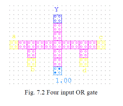
| Similarly, the five-input gate of Fig. 6 can also be used to form a four input OR gate as shown in Fig. 7.2. For this
configuration the input e is restricted to have a fixed polarity that is equal to 1. As for the AND gate, the selection of e
is unique. For the remaining cells, the same symmetry is present in the OR gate as in the previously described AND
gate. The function represented is Y=a+b+c+d. |
 |
SIMULATION RESULTS |
| With QCADesigner, the circuit functionality is verified. The following parameters are used for a bistable
approximation: Cell size 18nm, Number of samples 12800, Convergence tolerance 0.001000, Radius of effect 65nm,
Relative permittivity 12.9, Clock high 9.8e-22J, Clock low3.8e-23J, Clock amplitude factor 2, Layer separation
11.5nm, Maximum Iterations per sample 100. |
 |
 |
CONCLUSION |
| The logical structures such as AND and OR using five-input complex gate composed of a 3-input majority
gate have been designed. One of these inputs typically functions as control inputs to determine the logical structure
formed by the four other inputs to the circuit. This five-input gate can be configured as a four-input AND gate and a
four-input OR gate which are verified through simulation results. |
References |
- C.S.Lent, P.D.Tougaw, W.Porod, and G.H.Bernstein, âÃâ¬ÃÅQuantum cellular automataâÃâ¬ÃÂ, Nanotechnology, vol.4, no.1, pp.49âÃâ¬Ãâ57, January1993.
- P.D.Tougaw, C.S.Lent, and W.Porod, âÃâ¬ÃÅBistable saturation in coupled quantum-dot cellsâÃâ¬ÃÂ, Journal of Applied Physics, vol.74, no.5, pp.3558âÃâ¬Ãâ 3566, September1, 1993.
- S P.D.Tougaw and C.S.Lent, âÃâ¬ÃÅLogical devices implemented using quantum cellular automataâÃâ¬ÃÂ, Journal of Applied Physics, vol.75, no.3, pp.1818âÃâ¬Ãâ1825, February1, 1994.
- C.S.Lent and P.D.Tougaw, âÃâ¬ÃÅLines of interacting quantum-dot cells: A binary wireâÃâ¬ÃÂ, Journal of Applied Physics, vol.74, no.10, pp.6227âÃâ¬Ãâ6233, November15, 1993.
- S.Lent, P.D.Tougaw, and W.Porod, âÃâ¬ÃÅBistable saturation in coupled quantum dots for quantum cellular automataâÃâ¬ÃÂ, Applied Physics Letters, vol.62, no.7, pp.714âÃâ¬Ãâ716, February 15, 1993.
- C.S.Lent and P.D.Tougaw, âÃâ¬ÃÅA device architecture for computing with quantum dotsâÃâ¬ÃÂ, Proceedings of the IEEE, vol.85, no.4, pp.541âÃâ¬Ãâ557, April 1997.
- S.Karthigai Lakshmi, G.Athisha, âÃâ¬ÃÅEfficient design of logical structures and functions using nanotechnology based quantum dot cellular automata designâÃâ¬ÃÂ, International Journal of Computer Applications, vol.3, no.5, (0975-8887), June 2010.
- QCADesigner, version 1.3.2. Available at http://www.atips.ca/projects/qcadesigner/.
- K. Walus, T. Dysart, G. Jullien, and R. Budiman, âÃâ¬ÃÅQCADesigner: A rapid design and simulation tool for quantum-dot cellular automataâÃâ¬ÃÂ, IEEE Trans. Nanotechnology., vol. 3, no. 1, pp. 26âÃâ¬Ãâ29, Mar. 2004.
|