International Journal of Advanced Research in Electrical, Electronics and Instrumentation Engineering
ISSN ONLINE(2278-8875) PRINT (2320-3765)
ISSN ONLINE(2278-8875) PRINT (2320-3765)
| Mukesh P. Mahajan, Pramod S. Aswale and Vivek D. Ugale Assistant Professor, Dept. of ETC, SITRC, Nashik, Maharashtra, India |
| Related article at Pubmed, Scholar Google |
Visit for more related articles at International Journal of Advanced Research in Electrical, Electronics and Instrumentation Engineering
Nowadays application specific soft processor cores are gaining importance for FPGA based embedded application in which user can configure the processor as per requirement. The architectural simplicity of ARM processors makes them suitable for low power applications. Hardware description languages (HDLs) are commonly used to construct hardware system. FPGA provides reconfigurable platform, so reuse of the design is a common practice to improve the productivity nowadays. In this paper the data processing instructions of ARM processor are implemented using Very high speed integrated circuit Hardware Description Language (VHDL) language and verified by applying test bench on Xilinx’s Spartan III based FPGA.
Keywords |
| ARM, VHDL, FPGA, data processing instructions. |
INTRODUCTION |
| The Arm processor has large uniform register file, load/store architecture, where data-processing operations only operate on register contents, not directly on memory contents. Simple addressing modes, with all load/store addresses being determined from register contents and instruction fields only Uniform and fixed-length instruction fields to simplify instruction decode [5]. The ARM processor has been specifically designed to be small to reduce power consumption and extend battery operation.The ARM architecture gives Control over both Arithmetic Logic Unit (ALU) and shifter in every data-processing instruction to maximize the use of an ALU and a shifter Load and Store multiple to maximize data throughput. These enhancements to a basic RISC architecture allow ARM processors to achieve a good balance of high performance, small code size and low power consumption. [4] The FPGA based design reduces time to market & adds design flexibility and adaptability with optimal device utilization and conserving both less board space and system power, which is often not the possible in every case of ASIC chips. [3] In following this line of thought, this paper summarizes our recent progress in developing VHDL soft-core of ARM processor on Xilinx’s Spartan III based FPGA. An advantage of implementing a full-featured ARM processor soft-core on FPGA is complete hardware customization while implementing various applications. |
RELATED WORK |
| The hardware debugging technology is integrated in ARM processor so that programmers can view what is happening during execution of code by processor. With this programmers can resolve issues very quickly and reduce time to market and overall development cost. The ARM is not pure RISC architecture because of various limitations of applications in embedded system. Nowadays Speed is not major constraint but power consumption and cost effective solutions are also playing vital role [1] [2]. |
| In [1] ARM soft processor core were implemented in the context of FPGA based multiprocessor based SOC applications. All the 32-bit instructions were implemented with single cycle data path and random logic based instruction decoder. The instructions of Data processing, Arithmetic, Branch instructions, Logical and compare were implemented. The [2] proposed Virtual ARM Simulation Platform and discussed how it can be used to reduce design time and cost. |
SYSTEM MODEL AND ASSUMPTIONS |
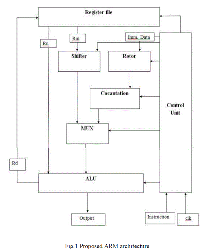
| The ARM architecture has been designed to allow every small and high-performance implementation. The architectural simplicity of ARM processors leads to very small implementations, and small implementations allow devices with very low power consumption. The ARM is a reduced instruction Set Computer (RISC), as it incorporates typical RISC architecture features. [5] The proposed architecture of the processor is shown in fig.1 |
| The main components of the proposed architecture are |
| 1. Register file which contains 16 register of 32 bits. |
| 2. Barrel shifter of capability to shift 32 bit right/left, arithmetic/logical. |
| 3. Rotor having capability to rotate 8 bit data right/left. |
| 4. Cocantation which convert 8 bit output of rotor into 32 bit. |
| 5. Multiplexer which select one of two 32 bit inputs. |
| 6. Arithmetic Logic Unit (ALU) to execute data processing instructions |
| 7. Control Unit which control all blocks according to instruction. |
 |
DATA PROCESSING INSTRUCTIONS |
| The proposed work implements data processing instructions of the ARM processor. The data processing instruction is only executed if the condition is true. The instruction format for data processing instruction is given below in fig.2. The instruction produces a result by performing a specified arithmetic or logical operation on one or two operands. The first operand is always a register (Rn). The second operand may be a shifted register (Rm) or a rotated 8 bit immediate value (Imm) according to the value of the I bit in the instruction. The condition codes in the CPSR may be preserved or updated as a result of this instruction, according to the value of the S bit in the instruction. |
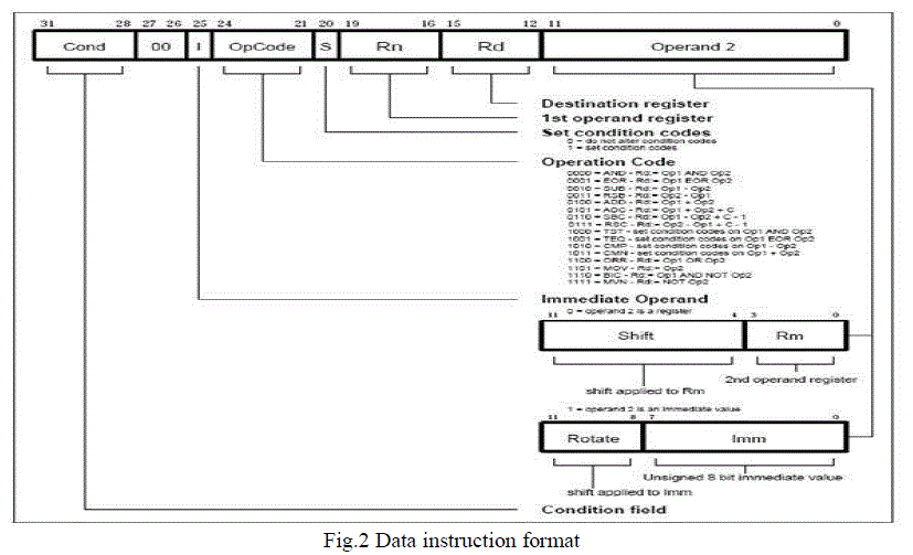 |
| Certain operations (TST, TEQ, CMP, CMN) do not write the result to Rd. They are used only to perform tests and to set the condition codes on the result and always have the S bit set. |
| The proposed instruction set is shown in fig.3 |
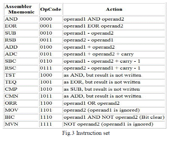 |
| It contains instructions following operations. |
| • Arithmetic operations. |
| • Comparisons. |
| • Logical operations. |
| • Data movement between registers |
| These instructions only work on registers not on memory. They each perform a specific operation on one or two operands. First operand is always a register Rn and second operand sent to the ALU via barrel shifter. |
IMPLEMENTATION & RESULT |
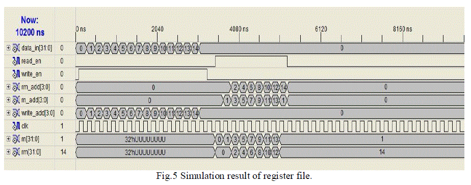
| 1. Register file |
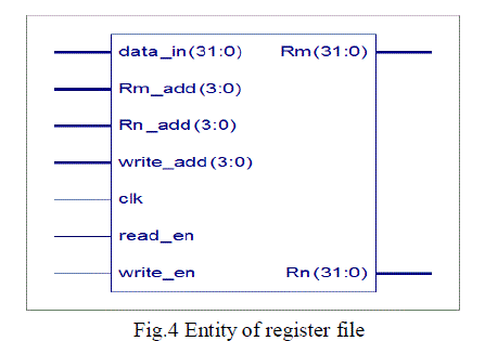 |
| It contains 16 register of 32 bits since we are using user mode, all register are accessible to user. The entity of register file and its simulation result are shown in fig.4 and fig.5. |
 |
| 2. Barrel shifter |
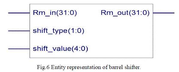 |
| The barrel shifter has a 32-bit input to be shifted. This input is coming from the register file. The shifter has other control inputs coming from control unit. Shift field in the instruction controls the operation of the barrel shifter. The fig.6 shows the entity representation of barrel shifter. |
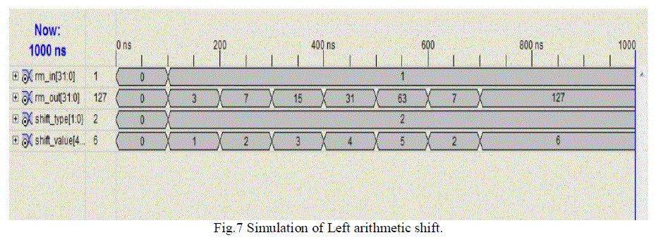 |
| The simulation result of barrel shifter for arithmetic left shift operation is shown in above fig. Similarly simulation results are achieved for right arithmetic shift |
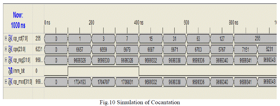
| 3. Rotor & Cocantation: |
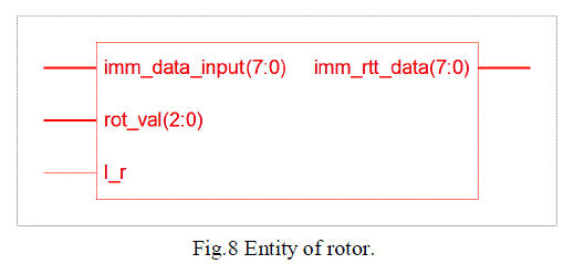 |
| The fig.8 shows entity of rotor. It is having capability to rotate 8 bit data right or left. The input is coming from immediate data contain in immediate field of instruction through control unit. The output of rotor is 8 bits; it is converted into 32 bit by Cocantation with null values |
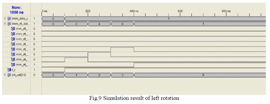 |
| The simulation result of rotor for left operation is shown in fig.9. The simulation results of Cocantation operation are shown fig.10. The simulation results are also achieved for Right rotation. |
 |
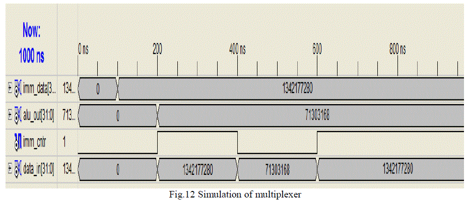
| 4. Multiplexer |
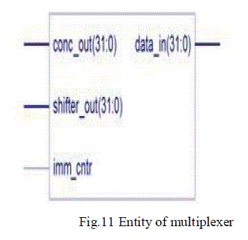 |
| It selects one of two 32 bit inputs coming from barrel shifter and Cocantation output, gives result to ALU. The entity representation of multiplexer is shown in fig. 11. It also performs to select data immediate from user or output of ALU data Rd to store back in register file. |
 |
| 6. Arithmetic Logic Unit (ALU) |
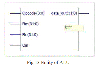 |
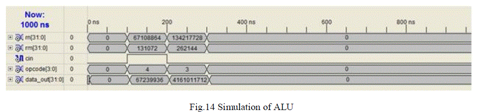
| The ALU has two 32-bits inputs. The first comes from the register file while the other comes from the shifter. ALU output is stored at Rd location in the register file. The ALU has a 4-bit function bus that allows up to 16 Opcode to be implemented. The different Opcode and their corresponding arithmetic and logic operations are performed on operands. The fig.13 & fig.14.shows the entity and simulation result for arithmetic logic unit. |
 |
| 7. Control Unit |
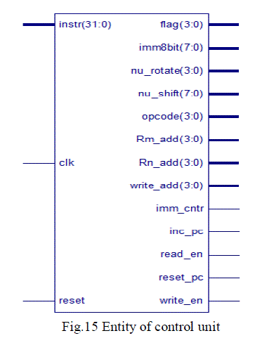 |
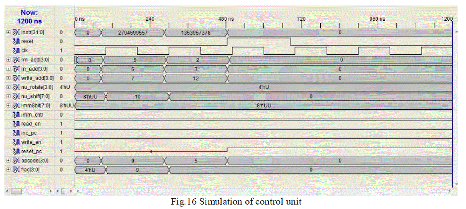
| The control unit fetches 32 bit instruction and provides control signals to the various the modules in the architecture. The controller provide outputs multiplexer controls, ALU functions, register reads /writes, flags, shift field, rotate value and other control signals to the hardware depending on the current instruction. The entity and simulation result is shown in fig.15 & fig.16. |
 |
| All the results are taken using Xilinx’s ISE 8.1i tool. The target device selected for the implementation is 3s500ecp132- 5 from family Spartan III. |
CONCLUSION AND FUTURE SCOPE |
| The data processing instructions of ARM soft-core processor were synthesized, simulated and implemented on Spartan III FPGA using Xilinx’s ISE tool. The code for all the modules were written using VHDL and tested by applying test benches. All the modules are working satisfactory as per expectation. In terms of future work, there are many possible areas to improve and do further development. So the ARM processor embedded into FPGA can be used for different applications like DSP and Image processing. The design can be embedded into high end FPGA devices for better performance. The reconfigurable ARM core can be used for verification platform in the industries. |
References |
|