Communication is the most important thing in this modern world, everyday new trends are emerging. Recently the immense demand for internet access and cellular services has led to the demand of communication standard which provides high data rate, coverage and mobility. WiMAX is becoming popular as an option for the last mile connection replacing cable modems and DSL connections. Specifically, WiMAX, the IEEE 802.16 standard came as a wireless MAN standard. But these communication channels are suppressed by burst error. The channel interleaver employed in the WiMAX transmitter plays a vital role in minimizing the effect of burst error. As per IEEE 802.16e standard this interleaver is explained by two permutation steps. But the implementation of these permutation steps is complex because of presence of floor function. Hence, in this approach simple and resource efficient algorithm is proposed to eliminate the requirement of floor function along with its mathematical background to implement the address generating circuit for WiMAX interleaver on FPGA.
Keywords |
| Interleaver; de-interleaver; FPGA; WiMAX |
I. INTRODUCTION |
| Mobile WiMAX is the most emerging trend in recent wireless communication technology. WiMAX is based on
wireless metropolitan area networking (WMAN) standards developed by the IEEE 802.16 group. WiMAX's main
objectives are to cover remote areas where cable connection is not feasible or expensive and for better coverage
especially for mobile networks where users are always moving than, and WiMAX is supported by IEEE802.16e-2005
Standards. |
| In digital communication burst error occur, a number of random error correction codes (ECCs) have been developed.
ECC is however, not efficient in combating bursts of errors. Interleaving is a process to rearrange code symbols so as to
spread bursts of errors over multiple code-words that can be corrected by ECCs. By converting bursts of errors into
random like errors, interleaving thus becomes an effective means to combat error bursts. Similarly at the receiver side
de-interleaver performs the reverse of interleaver. So the designing of efficient and simple interleaver architecture is
needed. |
| A Simple, resource-efficient algorithm based architecture for interleaver address generating circuit used in mobile
WiMAX transceiver is proposed here. The floor functions which are needed for interleaver are eliminated with their
mathematical background. |
| The paper is organized as follows: Related works for WIMAX interleaver and deinterleaver address generator is
discussed in section II. Section III explains the interleaving and de-interleaving technique of the mobile WiMAX
system. In Section IV an algorithm is proposed for interleaver address generator its mathematical background,
algorithms and verilog program are presented. Section V shows the simulation and synthesis result. Finally, this work is
concluded in Section VI. |
II. RELATED WORK |
| In [3] a novel and efficient technique is proposed to design finite state machine based WiMAX multimode
interleaver using hardware description language and the hardware model is implemented on FPGA. In [4] authors
proposed novel design for the hardware of the interleaver block used in IEEE 802.16e standard using pattern tracking
mechanism. Pattern tracking refers to comparing of addresses generated to obtain the relationships between the next consecutive addresses to implement the architecture. Here it is implemented for channel interleaver with only ½ code
rate. In [5] an algorithm based address generating circuit is proposed along with mathematical background, the
requirement of floor function is eliminated. Here the address generating circuit is designed for all permissible code
rates, modulation schemes and de-interleaver depths supported by IEEE802.16e. |
III. SYSTEM DESCRIPTION |
| The main objective of the communication system is to transfer an information bearing signal from source to
destination called sink through a communication channel, channel may be wired or wireless. |
| In Fig 1, it is shown that the mandatory blocks of WiMAX transceiver system. Data i.e., time-varying signal called
message Signal from the source is Scrambled on each burst to avoid the long sequence of 0’s and 1’s using randomizer.
The RS-CC encoder (channel encoder) consists of an FEC scheme the key idea of FEC is to transmit enough redundant
data to allow the receiver to recover from errors all by itself and then channel interleaver rearranges input data such that
consecutive data are spaced apart. The bit interleaved data are converted to a sequence of complex valued symbols
using mapper. OFDM symbols are constructed by IFFT. In the receiver, the blocks are organized in the reverse order
enabling the restoration of the original data sequence at the output. The block interleaver/deinterleaver structure, which
is used as a channel interleaver/deinterleaver in the WiMAX system, is described in Fig. 2. |
| Here address generator is a circuit it generates interleaver addresses according to the pre determined permutation
scheme, it generates both read and write addresses depending on the select line. The encoded data is stored in bit
addressable interleaver memory and according to the read addresses generated data is read out to get the interleaved
data. Similarly we can write the data into the interleaver memory according to the write addresses and data read out
continuously. |
| A. Interleaving in WiMAX system: |
| The interleaving is a technique of reordering the encoded data such that the adjacent bits now become nonadjacent. The
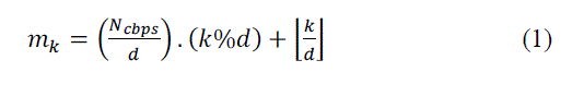
data stream received from the RS-CC encoder is permuted by using the two-step processes described by (1) and (2) [6].
These steps ensure mapping of coded bits onto nonadjacent subcarriers and alternate less/more significant bits of the
modulation constellation, respectively. Thus, |
 |
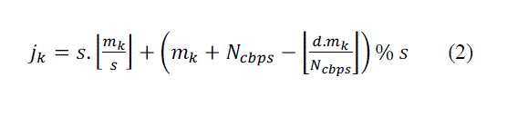 |
| Here, the number of columns is represented by (d= 16/12 for WiMAX) |
| In this project we have taken d=16, mk and jk are the outputs after the first and second steps, respectively;
Where: |
| k= 0, 1 . . . . . . Ncbps-1 |
| Ncbps=Number of coded bits per sub channel (it denotes the interleaver depth) |
| d =Number of columns (for WiMAX it is 16/12) |
| s=Ncbps/2, where Ncpc is the number of coded bits per subcarrier, i.e., 2, 4, or 6 for QPSK, 16-QAM, or 64-
QAM, respectively [6]. Modulo and floor functions are signified by % and⌊ ⌋, respectively. |
| B. Deinterleaving in WiMAX system: |
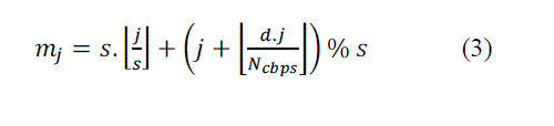
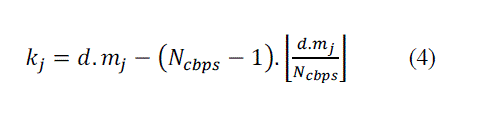
| The deinterleaver, which performs the inverse operation, is defined by two permutations steps, i.e., (3) and (4). Let
mj and kj define the first and second level of permutations for the deinterleaver, where j is the index of received bits
within a block of Ncpbs bits. As per[6], (3) and (4) perform inverse operation of (2) and (1), respectively. |
| Thus, |
 |
 |
| The block interleaver/deinterleaver supports different depths (Ncpbs) for all permissible code rates and modulation
Schemes (see Table I) for IEEE 802.16e [6]. |
| In this project we are concerned with the 3 modulation schemes, which are supported by WiMAX IEEE 802.16e. It
supports special modulation technique which is called Adaptive Modulation technique. |
IV. PROPOSED ALGORITHM FOR INTERLEAVER |
| Here, the algorithm proposed based on [5], for address generator of the WiMAX interleaver along with its
mathematical background has been described. A MATLAB program is developed using (1) and (2) for all modulation
schemes and code rates. Due to the presence of a floor function in (1) and (2), their direct implementation on an FPGA
chip is not feasible. Table II shows the interleaver addresses for the first four rows and six columns of each modulation type. As d=16 is chosen, the number of columns are fixed (=d) for all Ncbps, whereas the number of rows are given by
Ncbps/d. |
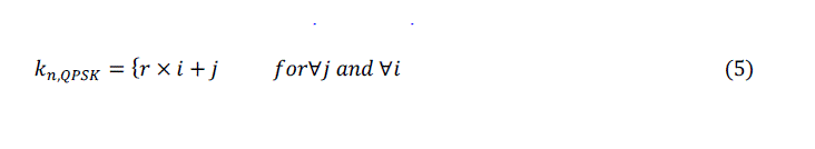
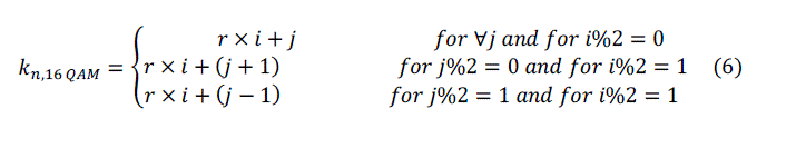
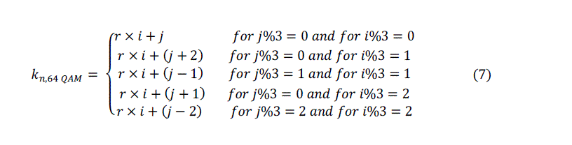
| A close examination of the addresses in table II confirms that the correlation between them follows the manner, as
shown in table III. The mathematical foundation of the correlation between the addresses, as derived in this brief, is
represented through (5)–(7) |
| Where: |
| i = 0, 1, 2 . . . , d-1 |
| j = 0, 1, 2 . . . , (Ncbps/d)-1 and |
| r = (Ncbps/d) represent row values. Here i and j represents the column and row numbers respectively. |
| From the algebraic analysis it has been proven that (5) – (7) represent the correlation between addresses of table III.
Thus (5) – (7) play the vital role in forming the mathematical background of our proposed algorithm. From the
correlation of table II and table III, and by mathematical representation of (5) – (7) three algorithms are proposed, these
algorithms eliminate the requirement of floor function in order to generate the interleaver addresses. |
| In below mentioned algorithm kn represents the interleaver addresses, “%” is the modulo function. |
 |
 |
 |
| The proposed algorithm is as follows: |
| A. QPSK: |
| Initialize Ncbps and d |
| for j=0 to (Ncbps/d)-1, j++ |
| for i=0 to d-1, i++ |
| kn= r*i+j |
| end for |
| end for |
| B. 16 QAM: |
| Initialize Ncbps and d |
| for j=0 to (Ncbps/d)-1, j++ |
| for i=0 to d-1, i++ |
| if (i mod 2) == 0) |
| kn = r*i + j |
| elseif (j mod 2)==0) |
| kn = r*i+(j+1) |
| else |
| kn = r*i+(j-1) |
| end if |
| end for |
| end for |
| C. 64 QAM: |
| Initialize Ncbps and d |
| for j=0 to (Ncbps/d)-1, j++ |
| for i=0 to d-1, i++ |
| if (i mod 3) == 0) |
| kn = r*i + j |
| elseif (i mod 3)==1) |
| if (j mod 3) == 0) |
| kn = r*i+(j+2) |
| else |
| kn = r*i+(j-1) |
| end if |
| elseif (i mod 3) == 2) |
| if(j mod 3) == 2) |
| kn = r*i+(j-2) |
| else |
| kn = r*i+(j+1) |
| end if |
| end if |
| end for |
| end for |
| Then these algorithms are transformed into MATlab programs and the addresses generated using these algorithms
are verified for the correctness of our algorithm with the results obtained from MATlab program for (1) and (2) for all
code rates, modulation schemes and all permissible interleaver depths of WiMAX interleaver. |
V. SIMULATION AND SYNTHESIS RESULTS |
| In order to test the proposed algorithms for the address generator of the WiMAX interleaver with all modulation
schemes and code rates, these algorithms are converted into verilog programs using Xilinx ISE 14.1 and the simulation
results are obtained from iSim 15.1 for all permissible code rates and modulation schemes. Simulation results are
verified with the previous MATlab results. Top level view of the complete interleaver address generator is shown in fig
3. And is synthesized for Xilinx Spartan-3E Starter board (Device XC3S500E) FPGA. And the same is implemented on
Spartan-3 (XC3S500E) Field Programmable Gate Array (FPGA). Simulation results are obtained for all permissible
modulation types and code rates using iSim and a part of the same for Ncpbs=192 bits, ½ code rate and 16-QAM has
been presented in Fig. 4. The initial portion of Fig. 4 shows the complete addresses for first row (j = 0), and the latter
part (from ruler) shows the addresses for second row (j = 1). The simulation results are verified with the output
obtained from the MATLAB program described in Section IV. Fig 5 shows the HDL synthesis device utilization
summary. |
| From the device utilization summary, our proposed architecture for interleaver design utilizes 6.78% slices, 2.70%
Slice flip flops and it utilizes two GCLKs which is 2% of the available GCLKs in Spartan-3E FPGA Starter board.
Minimum propagation delay and maximum operating frequency of the FPGA based interleaver is found to be 7.144ns
and 82.88MHz respectively. The interleaver address generator circuitry uses less FPGA resources; hence, it makes the
space for other associated circuitry like randomizer, encoder and mapper etc to be implemented on the same FPGA
chip. Because of the presence of floor and mod function in (1) and (2), direct implementation of the address generation circuitry is very complex and consumes large amount of logic resources. Instead, our algorithm based approach
provides a faster and resource efficient implementation of WiMAX interleaver on FPGA platform. |
VI. CONCLUSION |
| An algorithm along with its mathematical formulation, including proof for address generation circuitry of the
WiMAX channel interleaver supporting all possible code rates and modulation patterns as per IEEE 802.16e is
proposed. The algorithm is converted into an optimized digital hardware circuit. The hardware is synthesized for the
Xilinx Spartan-3E (Device XC3S500E) FPGA using Verilog and is implemented on Xilinx Spartan-3E starter board.
From the device utilization summary it is clear that it utilizes less FPGA resources. |
| |
Tables at a glance |
|
|
| |
Figures at a glance |
 |
 |
 |
 |
 |
| Figure 1 |
Figure 2 |
Figure 3 |
Figure 4 |
Figure 5 |
|
| |
References |
- W. Konhauser, âÃâ¬ÃÅBroadband wireless access solutionsâÃâ¬ÃâProgressive challenges and potential value of next generation,âÃâ¬Ã Wireless Pers.Commun., vol. 37, no. 3/4, pp. 243âÃâ¬Ãâ259, May 2006.H. Simpson, Dumb Robots, 3rd ed., Springfield: UOS Press, 2004, pp.6-9.
- B. Li, Y. Qin, C. P. Low, and C. L. Gwee, âÃâ¬ÃÅA survey on mobile WiMAX,âÃâ¬Ã IEEE Commun. Mag., vol. 45, no. 12, pp. 70âÃâ¬Ãâ75, Dec. 2007.
- B. K. Upadhyaya, I. S. Misra, and S. K. Sanyal, âÃâ¬ÃÅNovel design of address generator for WiMAX multimode interleaver using FPGAbased finite state machine,âÃâ¬Ã in Proc. 13th Int. Conf. Comput. Inf. Technol., Dhaka, Bangladesh, 2010, pp. 153âÃâ¬Ãâ158.
- Khater, M. M. Khairy, and S. E.-D. Habib, âÃâ¬ÃÅEfficient FPGA implementation for the IEEE 802.16e interleaver,âÃâ¬Ã in Proc. Int. Conf.Microelectron., Marrakech, Morocco, 2009, pp. 181âÃâ¬Ãâ184.
- Bijoy Kumar Upadhyaya and Salil Kumar Sanyal, âÃâ¬ÃÅEfficient FPGA implementation of address generator for WiMAXdeinterleaver,âÃâ¬Ã inIEEE Transactions on Circuits and Systems-II. Vol. 60, No. 8, pp. 492âÃâ¬Ãâ496, Aug. 2013.
- IEEE Standard for Local and Metropolitan Area NetworksâÃâ¬ÃâPart 16: Air Interface for Fixed Broadband Wireless Access Systems-Amendment 2, IEEE Std. 802.16e-2005, 2005.
- Xilinx Spartan-3 FPGA Family: Complete Data Sheet, Xilinx, Inc., San Jose, CA, USA, 2012.
|