Research & Reviews: Journal of Material Sciences
ISSN:2321-6212
ISSN:2321-6212
A. Tahiri *, M Idiri, A Hasnaoui and B Boubeker
Laboratoire d'Ingénierie et Matériaux (LIMAT), Faculté des Sciences Ben M’Sik Casablanca, Université Hassan II, Casablanca, Maroc
Received Date: 18/12/2017; Accepted Date: 27/02/2018; Published Date: 05/03/2018
DOI: 10.4172/2321-6213.1000213
Visit for more related articles at Research & Reviews: Journal of Material Sciences
In this work we performed a series of nanoindentation test on nanocrystalline (nc) tungsten (W) specimens, using Molecular Dynamics (MD) simulations and Embedded Atom Method (EAM). We studied the grain size effect in the range of 6 to 15 nm, with a penetration rate of 5 Å/ps and at room temperature 300 K. We found an increase in reduced elastic modulus Er and the Young elastic modulus E with the increase in grain size. On the other hand, we investigated the effect of the penetration velocity ranging from 3 Å/ps to 5 Å/ps. We found that the elastic modulus increases when the rate of penetration increases. The found results are in good agreement with the literature
Nanoindentation, Nanocrystalline tungsten, Molecular dynamics simulations, Grain size, Indenter velocity
Nanocrystalline materials, with grain size less than 100 nm, are known to possess some attractive properties, such as high yield and fracture strengths [1], improved wear resistance [2]. A lot of applications of nanocrystalline materials depend on grain size and temperature. Hariss [3] studied mechanical properties of polycrystalline tungsten at temperature ranging from 25°C to 950°C using nanoindentation. This method is widely used to obtain the elasticity modulus, hardness, and yield stress of nanocrystalline materials [4-7]. Nanoindentation is a method that uses an indenter with a known geometry to drive into a specific site of the specimen by applying an increased load [8,9]. This method is widely used for measuring mechanical properties of thin films, because it employs small loads (in the order of nanonewtons) that enable handling thicknesses at the nanometer scale. Recently some works are carried out using Finite Element (FE) nanoindentation simulation to study mechanical properties of thin films and coated systems [10,11]. Because of the development of computer simulation technology, the simulation scale expended from thousands to millions of atoms. Molecular Dynamics (MD) simulation has been used extensively to study material properties in various fields such as bioscience, chemistry, material science and technology [12,13]. Hasnaoui et al. [14] studied interaction between dislocations and grain boundaries under an indenter. Kelchner et al. [15] found that initial partial dislocation loops were nucleated off the indenting axis below the Au(111) surface. Ruestes [16] has studied the effects of indenter diameter, penetration velocity and interatomic potentials on defect mechanisms and evolution of tantalum nanoindentation. Hagelaar [17] studied the formation and destruction of nanoindentation contacts in tungsten. According to Li, et al. [4], MD simulations have been used to study the plastic deformation initiated by the indentation process. Dislocation nucleation and pile-up are observed during nanoindentation of a single crystal iron. Moreover, the plastic deformation of nanocrystalline tantalum during nanoindentation is regulated by deformation twin in terms of surface topography [18]. The main goal of this work is to analysis these effects on nanoindentation of nc tungsten by using MD simulations. The results are compared in part with those proposed by other simulation methods but also with experience.
Interatomic Potentials
The MD simulation solves NewtonÃÆâÃâââ¬Ãâà ¸s equations of motion and gives the trajectory of each atom in each time. The forces on an atom are computed as negative gradients of the potential energy of each atom [19]. The source of this potential energy is the interatomic potential, which limits the physics of how atoms interact with each other, and can be considered as the critical component of an MD simulation. An interatomic potential uses the location of an atom relative to all of its neighbors to calculate its potential energy. The mathematical form of an interatomic potential is typically selected and then parameters are determined by fitting to experimental and quantum mechanical simulation data; for this reason, potentials are considered to be empirical [20]. The embedded atom method is currently a common technique used in molecular dynamics computer simulation of metallic systems [21]. The method provides a good description of the interatomic forces in the system, particularly for fcc metals. It calculates the interatomic potentials in metals and models forces between atoms as follows
 (1)
(1)
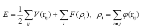
Where E is the total energy of the system, V(rij) represents the pair interaction energy between an atom i and its neighboring atom j, φ(rij) is the electronic density function, and F(ρi) represents an embedding function accounting for the effects of the free electrons in the metal [22]. In particular, we used the EAM potential functions developed [23].
In this study, MD simulations are performed using the Large Scale Atomic/Molecular Massively Parallel Simulator code (LAMMPS) [24]. We use periodic boundary conditions in the lateral directions (x and y) and a free surface in the indenting direction (z). The sample sizes perpendicularly to the indentation direction were chosen to be large enough to avoid spurious effects of the periodic boundary conditions. We used a fixed boundary condition at the bottom of the nc-W, representing a hard substrate. The indenter is modeled by a virtual spherical indenter using a strong repulsive potential.
Sample Preparation
We start by constructing nanocrystals that contain 5 grains with anaverage grain size of 15 nm, 9 nm and 6 nm using the Voronoi construction [25]. The simulations box is a cube with dimensions corresponding to the average grain size. The heart of the grains contains atoms are ranging bcc lattice with random crystallographic orientations. The simulations were performed using a rigid spherical indenter with a radius of 30 Å. The indenter moved toward the surface of the sample at a constant velocity until the desired depth was reached and then the system was equilibrated for several simulation steps [26,27].
Indentation Simulation Process
In this work we use an indenter velocity ranging from 3 Å/ps to 5 Å/ps, which is much faster than in experiments [28], but although carried out with relatively higher speed these simulations could still reveal the main features of the atomic rearrangements [29]. The MD time step is set to 1fs. The sample was initially relaxed at 300 K using the velocity rescaling method [4]. The bottom 20 Å of the substrate are kept fixed; the region from 20 Å to 40 Å are set as the thermostat atoms and the top of the sample surface was treated as a free surface [30].
Hertzian Contact
Figure 1 exhibits an example of the load curves that shows the load versus the indentation depth for a grain size of 15 nm. The indenter force was determined from an average of the instantaneous indenter force over the last 100 fs before the indenter is moved down. The force in hertzian theory is given by:

Figure 1: The load vs. indentation depth curve fitted on the Hertzian theory.
 (2)
(2)
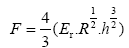
Where R stands for the radius of the indenter (30 Å), h is the indentation depth and Er is the reduced elastic modulus of W, given by:
 (3)
(3)
With E is the Young’s modulus and ϑ the PoissonÃÆâÃâââ¬Ãâà ¸s ratio. We note that the value of is taken to be 0.28 as given by the interatomic potential [26].
We can see from Table 1 that the Young’s modulus increases with increasing of the grain size. On the other hand, the Young modulus value 399.3 GPa, found for the 15 nm grain size sample is close to that of bulk W (410 GPa) [31]. Kang et al. [32] obtained value of 323.6 GPa for the Young modulus by nanoindentation and nanoscratch experiments of polycrystalline tungsten. Hariss et al. [3] carried out experiments and found that the reduced elastic modulus value is 287 GPa for the temperature range from 25 to 800°C. At 300 K, we calculated reduced elastic modulus of the 6nm average grain size sample and found 318.1GPa. This result is very close to that found experimentally by Dylan et al. [33] (317 GPa).
Table 1: Values of reduced elastic modulus, Young’s modulus of nc-W.
| Mechanical properties | 6 nm | 9 nm | 15 nm |
|---|---|---|---|
| Reduced elastic modulus (Er) in GPa | 318.1 | 334.6 | 433.3 |
| Young modulus in GPa | 293.2 | 308.3 | 399.3 |
Reduced Elastic Modulus
We plotted the result of Table 1 in Figure 2 and observed that the reduced elastic modulus Er of nanocrystalline tungsten shows a linear relationship with the reciprocal average grain size 1/d. This behavior has been observed experimentally by Sanders et al. [34].

Figure 2: The linear relationship between Er and 1/d.
The linear relationship between Er and 1/d may be a general feature for nanocrystalline metals in the average grain size ranging presented in this paper. When the average grain size decreases the atomic fraction in grains boundary will decrease because of the increase of atomic fraction in grains. This can be seen in Figure 3, which shows that the reduced elastic modulus increases almost linearly with increasing of the atomic fraction of grains. We can deduce that Er and 1/d have a linear relationship, at least in the studied range of average grain size. Zhou and Nan [35] also found a linear relationship for nanocrystalline metals with body-centered cubic (bcc) structure [35].

Figure 3: Reduced modulus Er various atomic fraction of grains.
It is important to study the effects of the velocities of the indenter on the mechanical behavior. The velocities of the indenter are varied from 35 Å/ps to 5 Å/ps, respectively. In Figure 4, we plotted an example of these curves for the penetration velocity of 5 Å/ps. We found that for 5 Å/ps, the slope of the load–depth curve (10 eV.Å-3) is steeper than that for the 4 Å/ps (8.9 eV.Å-3) and 3Å/ps (8.3 eV.Å-3). This shows that the Young’s modulus increases with the penetration velocity. These results were also found for nc-Ni [28] and nc-Cu [36].

Figure 4: Load- displacement curve for indentation velocities of 5 Å/ps and a grain size of 6 nm.
MD simulations have been used to study the effect of penetration velocity and grain size on reduced elastic modulus and Young’s modulus of nanocrystalline tungsten. The load-depth curve is in a good agreement with the modified Hertizian theory. The values of the reduced elastic modulus obtained agree well with experiment and finite element simulation results. The effect of indentation velocity showed that the reduced modulus Er increases as the penetration velocity increases. The reduced modulus Er shows a linear relationship with the reciprocal of average grain size 1/d for nanocrystalline tungsten. This behavior is explained by the increase of the fraction of grain boundary atoms when the grain size increases.